What is the role of the differential amplifier circuit in increasing the input resistance?
(a) emitter bias difference
(b) current source bias difference
A differential amplifier circuit has two input terminals and two output terminals, allowing for both double-ended and single-ended signal configurations. In a double-ended input setup, the signal is applied to both inputs simultaneously, while in a single-ended input configuration, the signal is applied between one input and ground, with the other input grounded. Similarly, for outputs, a double-ended output takes the signal between the two outputs, whereas a single-ended output takes the signal from one output to ground. As a result, the differential amplifier can operate in four modes: double-ended input with double-ended output, single-ended input with double-ended output, double-ended input with single-ended output, and single-ended input with single-ended output. The circuits discussed here are in the double-ended input and double-ended output mode.
**Input Resistance Analysis of Differential Amplifier Circuit**
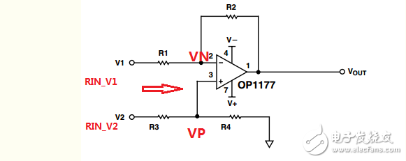
*Figure 1: Classic differential circuit input resistance analysis*
Assuming the following conditions:
1. The op-amp is ideal.
2. Resistors are matched, with R1 = R2 = R3 = R4 = 10kΩ.
Let RIN_V2 and RIN_V1 represent the input resistances seen at the V2 and V1 terminals, respectively.
As shown in Figure 1, the input resistance at the V2 terminal is straightforward: RIN_V2 = R3 + R4. Since no current flows into the op-amp's input terminals, we have:
RIN_V2 = R3 + R4 = 20kΩ
Now, focusing on RIN_V1:
Suppose a signal V1 is applied to the V1 terminal, and a current I is generated at that input. The input resistance RIN_V1 can be expressed as:
RIN_V1 = U / I
From the circuit diagram, we derive:
I = (U - VN) / R1
VN = VP = V2 * R4 / (R3 + R4)
Substituting these equations, we get:
RIN_V1 = V1 * (R3 + R4) * R1 / [V1 * (R3 + R4) - V2 * R4]
Further simplification leads to:
RIN_V1 = [2K2 - K1(R3 + R4) * R1] / [(2K2 - K1)(R3 + R4) - (2K2 + K1)R4] --- (20)
Where:
K1 = V2 - V1 (differential signal)
K2 = (V2 + V1)/2 (common-mode signal)
From equation (20), it’s clear that RIN_V1 depends on resistor values, the differential signal, and the common-mode signal.
Consider a simple case where the common-mode voltage VOCM is zero, i.e., K2 = 0.
Substituting into equation (20):
RIN_V1 = K1*(R3 + R4)*R1 / [K1(R3 + R4) + K1*R4]
= (R3 + R4)*R1 / (R3 + 2*R4)
= 6.666kΩ
In summary:
1. The performance of an op-amp-based differential circuit depends on the op-amp quality and resistor matching, so multiple factors must be considered during design.
2. The input resistances at the two input terminals are often unequal, which can affect the overall performance of the differential amplifier.
It is precisely because of these limitations that more advanced differential amplifiers and instrumentation amplifiers were developed to improve accuracy and performance.
Low Frequency Transformer
Constant Voltage Transformer,Laminated Transformer,Encapsulated Transformer,12V Ac Transformer
IHUA INDUSTRIES CO.,LTD. , https://www.ihuagroup.com