Quad Channel Power Management IC PCB Layout Guide for Vehicle Power Supply
introduction
A reasonable PCB layout is critical, especially in the design of high frequency switching regulators such as the MAX20021/MAX20022. The optimized PCB layout provides clean output and simplifies debugging in electromagnetic interference (EMI) testing. This article describes some of the key areas of optimizing circuit layout to ensure optimal performance.
Overall layout design guide
Keep the loop area formed by the input capacitors (C5-C8), inductors (L1-L4), and output capacitors (C1-C4) to a minimum.
Place the VA output capacitor (C9) as close as possible to pin 26 (VA and pin 24 (GND). Do not have a via between the capacitor and the pin. This pin is the analog supply input to the IC and any inductors generated on the leads. Both will increase the analog noise, which will increase the output jitter of LX[1:4].
Use the shortest possible route.
Optimize AC-DC current path
To reduce electromagnetic emissions, the passive component layout around the MAX20021/MAX20022 is critical. The path in which the current step changes is called the AC path and occurs at the moment when the switch is turned on/off. After the switch is turned ON/OFF, the path through which the current flows is a DC path.
Communication path
The MAX20021 synchronous rectification dc-to-dc converter has three passive components (C1, C5, L1) on the output current path of each output. These three components have a significant impact on electromagnetic radiation and device performance. Figure 1 and Figure 2 show the switching current path of OUT1 during ON/OFF. Figure 3 shows the difference between the two current paths with the maximum di/dt. The C5 wiring should be prioritized, followed by the L1 and C1 wiring.
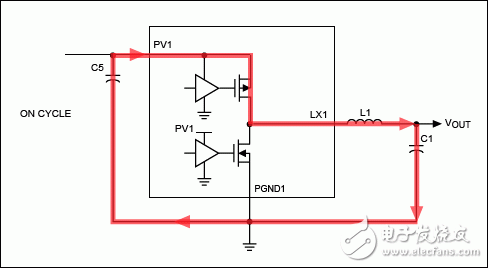
Figure 1. Current path for OUT1 when the PMOS is on.
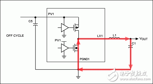
Figure 2. Current path for OUT1 when DMOS is on.
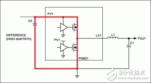
Figure 3. OUT1 AC path differences.
Spread spectrum
If the improved wiring cannot pass the user's radiation standard test, the MAX20021/MAX20022 products with clock spread spectrum can be customized. The spread spectrum device can reduce the noise of the FM band by 12dB compared with the standard version. Refer to the device data sheet for instructions on customizing the spread spectrum device.
We are amongst the trusted manufacturer, supplier & exporter of premium quality range of Solar LED Street Lights.
These solar Led Street Lights are highly efficient and very economical systems for lightning different places. Our solar LED Street Lights are ideal for outdoor applications designed to efficiently harness solar power and store for use during night time.
We offer very robust, long lasting and very bright solar lighting systems to our clients at economical prices.
With the support of our skillful professionals, we offer our customers a high quality 12W LED Panel Light Square. Perfect for both indoor and outdoor purposes, offered square light is perfectly designed to meet the requirements of patrons.
120W Integrated Solar Street Lights
120W Integrated Solar Street Lights,120W Smart Solar Street Light,120W Solar Street Lights,120W Integrated Solar Street Lamp
Yangzhou Bright Solar Solutions Co., Ltd. , https://www.solarlights.pl