STMicroelectronics Releases Pressure Sensor Technology
 A few days ago, STMicroelectronics released a new patented technology that incorporates a self-contained sensor unit in a fully compression molded package.
 This proprietary technology enables the integration of a standalone pressure sensing cell in a fully compression molded package, enabling fully encapsulated wire bonding without the risk of corrosion, and preventing pick and place equipment from damaging wire bond points during chip assembly. There is no risk of capacitor separation or capacitor damage in the packaging process, and no influence on the sensor during the soldering process to ensure that the packaging solution is more rugged.
According to the research report of market analysis company Yole Développement, the MEMS pressure sensor market will grow from 1.9 billion U.S. dollars in 2012 to 3 billion U.S. dollars in 2018. The output of MEMS pressure sensors used in consumer electronics, especially smart phones and tablets, will reach 1.7 billion, surpassing MEMS's largest target market - automotive electronics applications. The global MEMS pressure sensor market will grow at a compound annual growth rate of 8 %. STMicroelectronics has more than 800 MEMS-related patents and patent applications globally. As the world's largest manufacturer of MEMS products, STMicroelectronics has MEMS production capacity of 4 million units and MEMS sales volume of more than 3 billion units.
Benedetto Vigna, executive vice president and general manager of Analog Devices, MEMS and sensor products at STMicroelectronics, said: “This technology represents a revolutionary improvement in performance and quality for pressure sensors. STMicroelectronics pioneered mass production of accelerometers and gyroscopes. We use the no-silicon full-compression package in the instrument. We are the first MEMS manufacturer to use high-precision and high-precision pressure sensors with no-silicon full-pressure encapsulation technology. Now we are using this technology in emerging pressure sensors. The field leads a revolution in packaging technology.
The new technology improves measurement accuracy (±0.2 mbar) while continuing to provide zero drift, low noise (0.010 mbar RMS) and a simplified calibration system that makes it particularly suitable for a wide range of consumer electronics, automotive and industrial applications, including indoor and outdoor navigation, location Services, enhanced GPS dead reckoning, altimeters and barometers, weather forecasting equipment and medical fitness equipment.
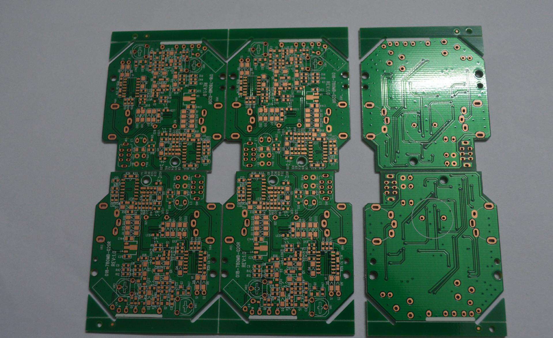
Organic Solderability Preservative is a cheap surface treatment.This surface treatment can protect the PCB Board surface and facilitate PCB Assembly. Its advantage is that it is easy to weld.this kind of PCB boards need to complete PCB assembly within three months. The board thickness from 0.2 mm to 6.0 mm, size from 5*5 mm to 600*650 mm can use the surface treatment of organic solderability preservative(Short name is OSP)

Organic Solderability Preservative
Organic Solderability Preservative,Organic Solderability Preservatives,Pcb Board Organic Solderability Preservatives
Orilind Limited Company , https://www.orilind.com