SEMI releases 8 new technology standards
SEMI has released eight new technology standards for the semiconductor, MEMS, FPD and photovoltaic manufacturing industries. These new standards were developed by equipment materials suppliers and device manufacturers' technical experts who participated in the SEMI International Standards Project.
These new standards are:
SEMI T20.3, Service Communication Specification for Semiconductor and Related Product Identification
SEMI E158, Mechanical Specifications for Wafer Transfer Equipment for Transfer and Storage of 450mm Wafers
SEMI M76, 450mm polished monocrystalline silicon wafer development specification
SEMI D60, FPD Polarized Film and Test Method for Scratch Resistance Characteristics of Materials
Mechanical specification for SEMI E156, 450mm wafer storage transfer interface
SEMI E157, Specification for Module Process Tracking
SEMI D59, 3D display terminology
SEMI PV4, Specification for the Fifth Generation Substrate Size Range for Thin Film Photovoltaics
Edit: Pony
High Precision Multilayer PCB|multilayer printed circuit board
Product name:
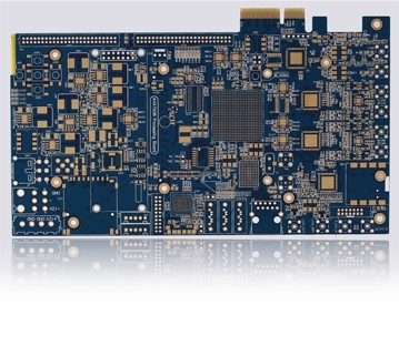
Industrial control board
Characteristic:
1, the board design
integration is very high;
2, the need to use composite
surface treatment method, gold finger plating hard gold 30 uinch;
3, gold finger position plate
thickness tolerance 1.6mm+/-0.10mm, it is recommended that customers in the
design of the gold finger corresponding to the inner line of the copper block,
in order to facilitate the plate thickness tolerance control.
Specifications:
Layer count: 6
Board thickness: 1.60mm
Base materials: FR4 S1141
Finished size: 172*148mm
Surface finish: Gold Plated +
finger
Line width/line space: 5/5mil
Minimum hole: 0.25mm
Solder resist color: blue
Cu thickness: inner layer 1 OZ
outer layer 1 OZ
Product name:
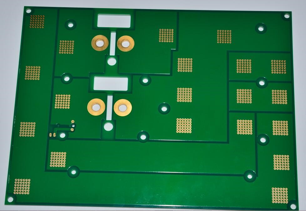
Thick Copper Board
Characteristic:
Prominent features: the outer
layer of copper thickness of 6 OZ, the inner product of copper thickness 6 OZ,
commonly used in large power equipment.
Processing difficulties:
1, inside and outside the need
to increase the thickness of copper thickness of 2 OZ or more by electroplating
method;
2, before pressing the need to
fill in the inner layer of resin;
3, the inner and outer layer
circuit is difficult to etch;
4, solder resist the need for
multiple printing.
 Specifications:
Layer count: 4
Board thickness: 3.0mm
Base materials: FR4 S1000-2
Finished size: 175*104mm
Surface finish:
Line width/line space:
12/12mil
Minimum hole: 0.5mm
Solder resist color: Sensitive
green
Cu thickness: inner layer 6 OZ outer layer 6 OZ
Product name:
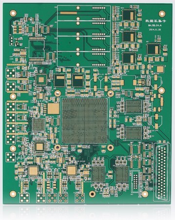
Data acquisition board
Characteristic:
1, the integration of the
board design is very high, thick diameter ratio of more than 10:1, heavy copper
plating is difficult;
2, the use of TG 170 plate
production.
Specifications:
1, the integration of the
board design is very high, thick diameter ratio of more than 10:1, heavy copper
plating is difficult;
2, the use of TG 170 plate
production.
Layer count: 8
Board thickness: 4.0mm
Base materials: FR4 S1000-2
Finished size: 400*400mm
Surface finish: mmersion
Line width/line space: 5/5mil
Minimum hole: 0.35mm
Solder resist color: Sensitive
green
Cu thickness: inner layer 1 OZ
outer layer 1 OZ
About Us:
BentePCB is a professional PCB manufacturing which is focus on double side, multilayer, HDI PCB , rigid PCB and Flexible PCB mass production. The company was established on 2011.
We have two factories together, The factory in Shenzhen is specialized in small and middle volume orders and the factory in Jiangxi is for big volumn.
Why Us?
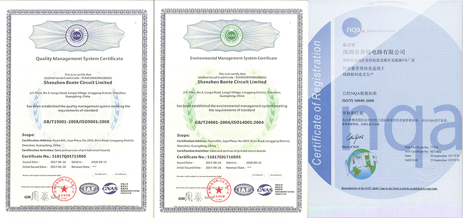
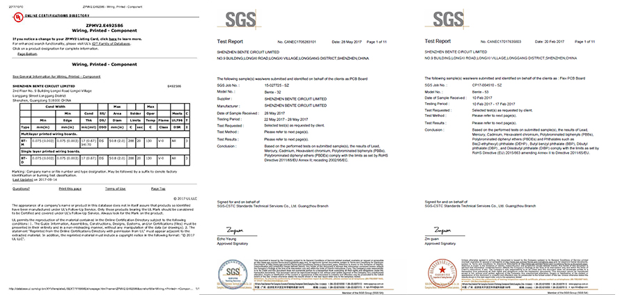
UL (E492586), ISO9001, ISO14001, TS16949, RoHS certified.
Turnover USD 10-50 million per year.
15,000 sqm area, 450 staff .
Mass Production from single to 16 layers.
Special Material:ROGERS, Arlon, Taconic.etc.
Client:Huawei, SAMSUNG, Malata, Midea,Texas Instruments.etc.
Certification(UL:E492586, TS16949, ISO14001, ISO9001,RoHS):
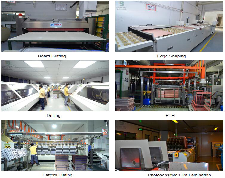
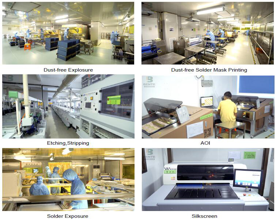
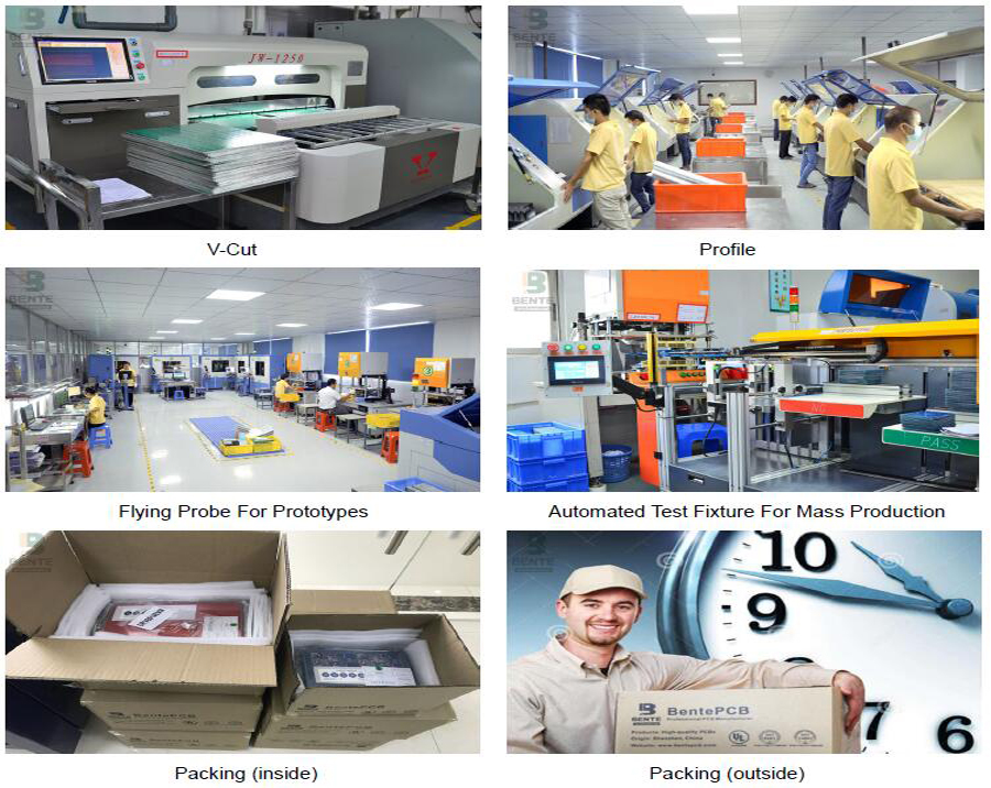
Factory Tour:
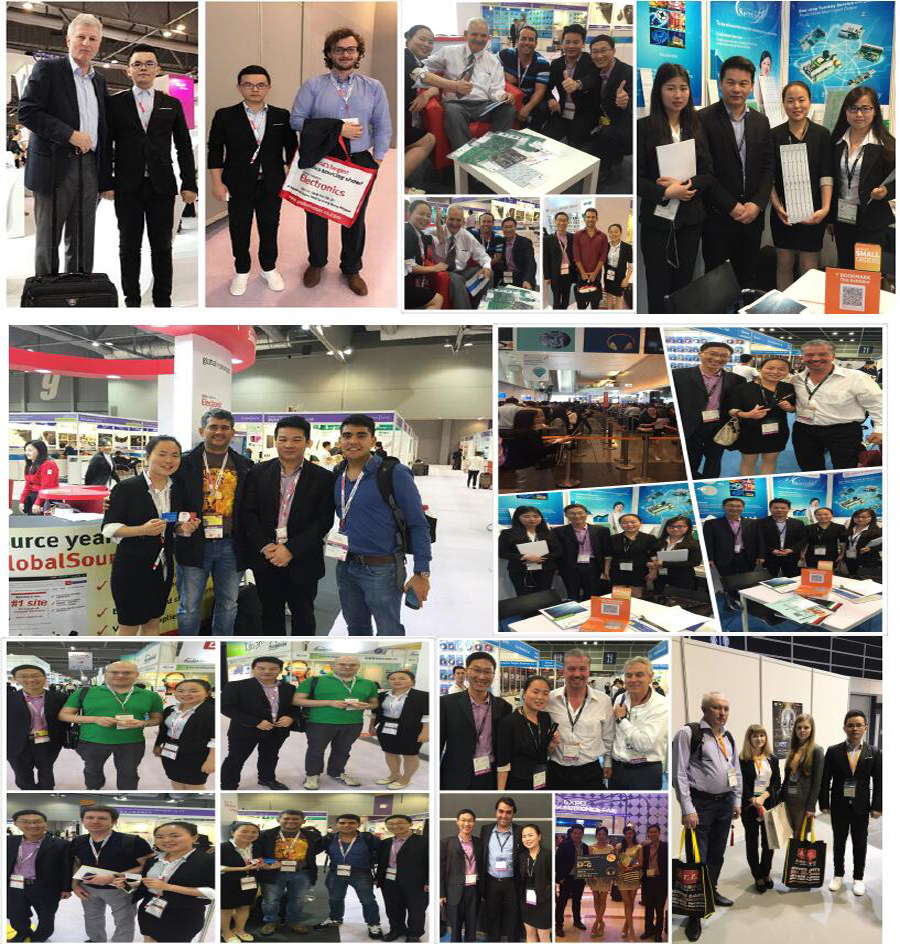
Exhibition:
We Took part in the famous exhibitions over the past years,and got highly appreciation from the top experts,as well as cooperated tightly with them.
Delivery:
BentePCB offers flexible shipping methods for our customers, you may choose from one of the methods below.


We don`t just sell PCBs .We sell sleep.

High Precision Multilayer PCB
High Precision Multilayer PCB, Multilayer Printed Circuit Board, Half Hole High-Precision Multilayer Board, High Precision Multilayer Board
Shenzhen Bente Circuit Limited , http://www.bentegroup.com