Buck switch regulator and three different operating modes
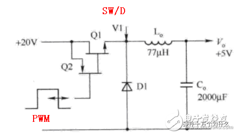
First, Buck Switch Regulator:
Second, CCM and DCM Definition:
1. CCM (Continuous Conduction Mode): Continuous conduction mode means that the inductor current never drops to zero during a switching cycle. The inductor is never "reset," meaning the magnetic flux doesn't return to zero during the cycle, and there's always current flowing through the inductor when the power switch is on.
2. DCM (Discontinuous Conduction Mode): Discontinuous conduction mode occurs when the inductor current reaches zero during the switching cycle. This means the inductor is fully "reset," and the inductor current is zero when the power switch turns on.
3. BCM (Boundary Conduction Mode): Also known as Critical Conduction Mode (CRM), this mode is where the controller monitors the inductor current. Once it detects the current reaching zero, the power switch is immediately turned on. The controller waits for the inductor current to reset before activating the switch again. If the inductor current is high and the ramp is flat, the switching period increases, making BCM a variable-frequency system.
Figure 1 shows the three different modes of operation using the inductor current waveform.
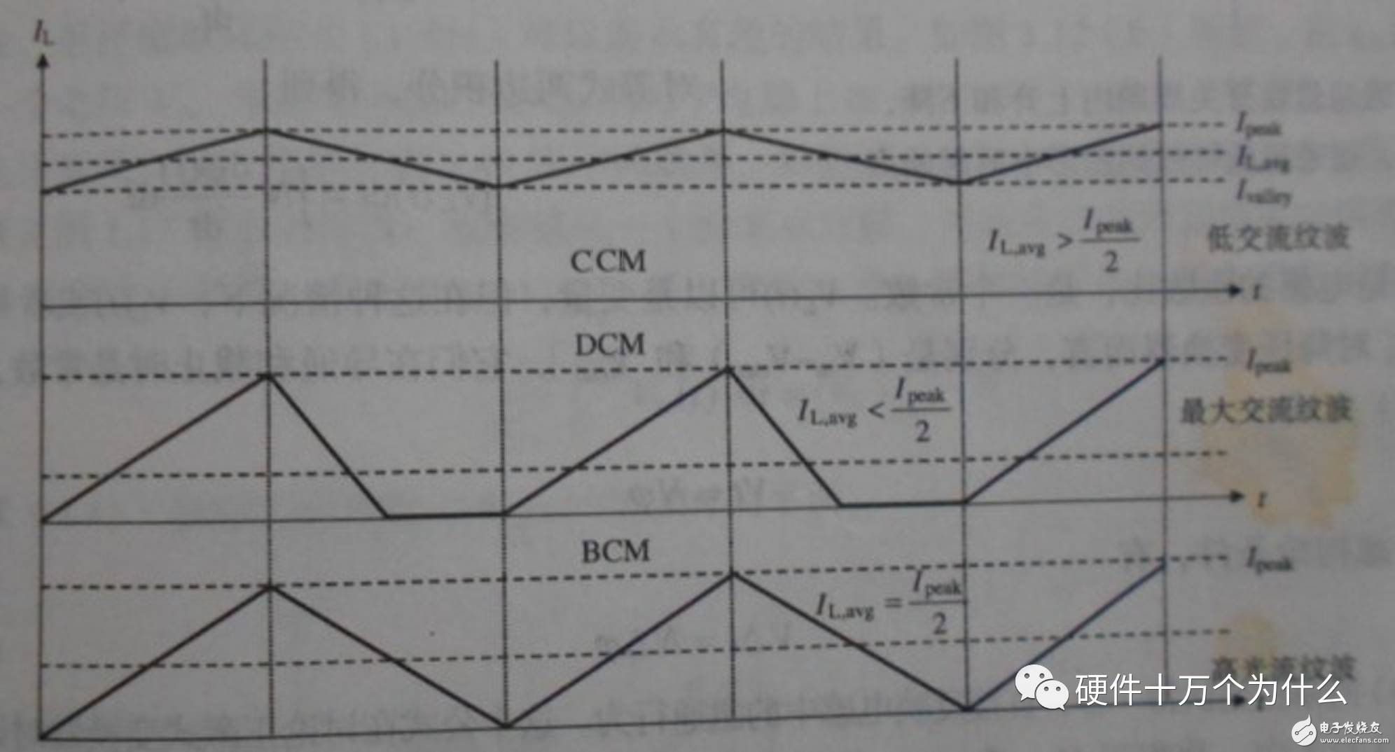
Figure 2: Three modes of inductor operation—CCM, DCM, BCM.
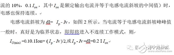
The midpoint amplitude of the current ramp equals the DC output current. The average value is shown in Figure 3, while the valley current is shown in Figure 4. The difference between them is the ripple current.


Third, CCM Operation Mode and Characteristics:
According to the CCM definition, the waveform of a buck converter operating in continuous mode is shown in Figure 3 below.
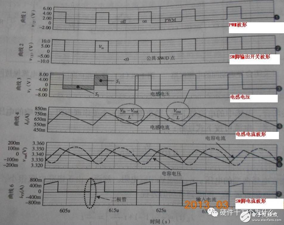
Image 3
Waveform 1 represents the PWM pattern, which triggers the switch to turn on and off. When the switch SW is on, the voltage at the common point SW/D is Vin. When the switch turns off, the common point SW/D voltage swings negatively, and the inductor current provides a bias current to the diode D, resulting in a negative buck-free-wheeling action.
Waveform 3 describes the change in inductor voltage. At equilibrium, the average inductor voltage L is zero, so S1 + S2 = 0. S1 corresponds to the product of voltage and time when the switch is on, and S2 corresponds to the product of voltage and time when the switch is off.
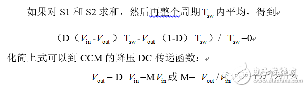
From the above formula, it can be seen that the result varies with D (duty cycle). Ideally, the transfer characteristics are independent of the output load. However, this description isn't entirely accurate. I'll explain it more clearly after reviewing the details carefully.
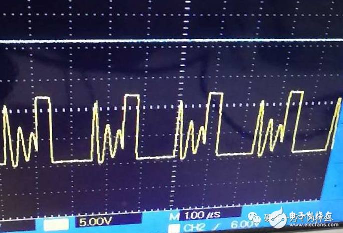
In reality, looking at the last waveform, when the switch is closed, the SW/D point current waveform has a large spike. I've measured the voltage waveform myself using the ACT4065 and ACT4065A chips, as shown in Figures 4 and 5. The reasons are as follows:
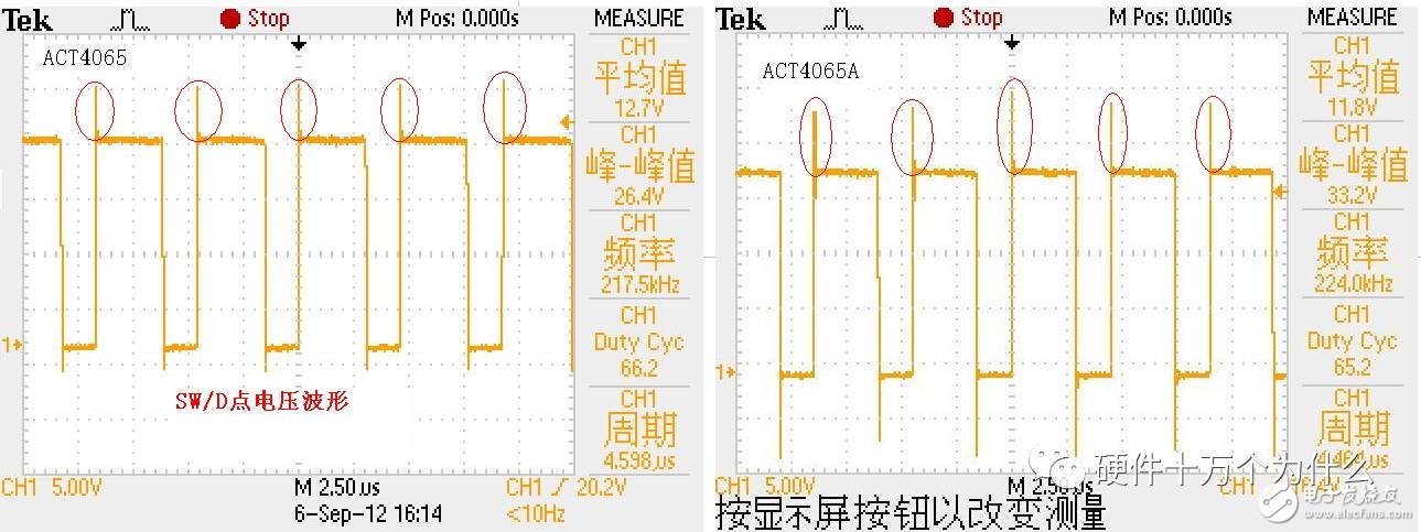
Figure 4, Figure 5
First, because the switch closes, it suddenly interrupts the conduction period of the diode. For a PN junction diode, it needs time to return to an electrically neutral state before it can conduct forward. During this recovery time, the diode exhibits short-circuit behavior before fully turning off. Schottky diodes don't have this recovery effect, but they do have large parasitic capacitance and junction capacitance. When the diode turns on, the SW quickly passes through the discharge capacitor, causing a current spike. Slowing down the switch turn-on time helps reduce the spike current.
Second, the shape of the current waveform also plays a role. As shown in the image, the output ripple (capacitor current waveform) is small, smooth, and has no pulse, indicating that the output current signal is well accepted by subsequent circuits, resulting in less power supply pollution. Additionally, the input current not only has spikes but also looks like a square wave. If the inductance L approaches infinity, the input current waveform becomes a real square wave, which is a pulsating current containing a lot of contamination, harder to filter than a typical sinusoidal current.
Square wave: consists of odd harmonics of a sine wave, i.e., frequencies 1, 3, 5, 7...n.
There are also spikes at the moment the switch turns off, likely due to the parasitic capacitance and junction capacitance of the diode and SW pin.
Through the above, the characteristics of the CCM buck regulator can be summarized:
1. D is limited to less than 1, so the output voltage of the buck converter is always lower than the input voltage;
2. If various ohmic losses are ignored, the transfer coefficient M is independent of the load current;
3. By adjusting the duty cycle D, the output voltage can be controlled;
4. The buck converter in CCM brings additional losses, as the freewheeling diode’s reverse recovery time consumes energy, adding burden to the power switch;
5. The output has no pulse ripple, but the input current is pulsed.
Fourth, DCM Operation Mode and Related Features:
The switching device operates in CCM when the load current is high, but when the load current decreases, the ripple current also decreases overall, as shown in Figure 2. When the load current drops to half the peak-to-peak value of the harmonic, the lowest point of the ramp just reaches zero, meaning the inductor current is zero and stores no energy. If the inductor current continues to decrease, the inductor enters DCM mode, and the voltage and current waveforms change significantly, as shown in Figure 6, with a significant change in the transfer function.
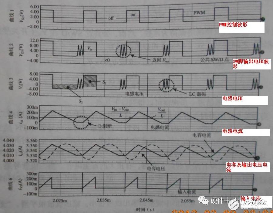
Figure 6
From waveform 4, it can be seen that the inductor current drops to zero, causing the freewheeling diode to turn off. If this happens, the left end of the inductor becomes open. In theory, the voltage at the left end of the inductor should return, since the inductor no longer has current and does not oscillate. However, due to the presence of many parasitic capacitances around it, such as the parasitic capacitance of the diode and SW, an oscillating circuit is formed. Like curve 2 and curve 3, a sinusoidal signal appears and disappears after several cycles, related to resistance damping. However, actual tests may differ. For example, in the ACT4065A test, the SW/D waveform was tested, but the oscillation occurred in the middle, as shown in Figure 7. The supplier engineer said this is in DCM mode, but I couldn’t find relevant information to verify.
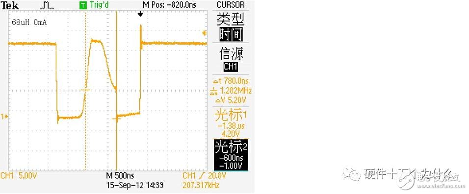
Figure 7
The Buck transformer controls the output voltage to a constant value over the entire load range, even if the inductor enters a discontinuous mode. Therefore, it's easy to mistakenly think that the inductor entering DCM mode has no effect on the circuit. In fact, the transfer function of the whole circuit changes, and the control loop must adapt to this change.
For the Buck regulator, there's nothing wrong with the inductor entering a discontinuous mode of operation. The DC output voltage before entering DCM is given by:

Note that this formula is independent of the load current parameter, so when the load changes, the duty cycle D doesn’t need to be adjusted, and the output voltage remains constant. In reality, when the output current changes, the on-time will also change slightly, as the turn-on voltage drop and inductance of Q1 change slightly with current, requiring Ton to make appropriate adjustments.
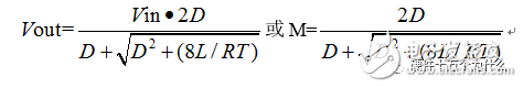
After entering DCM operation, the transfer function changes. The CCM transfer function no longer applies, and the switch on-time decreases as the DC output current decreases. The following is the transfer function in DCM mode, where the duty cycle is related to the load current, i.e.,
Because the control loop aims to keep the output voltage constant, the load resistance R is inversely proportional to the load current. Assuming Vout, Vin, L, T, and other parameters are constant, to maintain a constant voltage, the duty cycle must vary with the load current.
At the critical transition current, the transfer function transitions from CCM to DCM. When operating in CCM, the duty cycle remains constant and doesn't change with the load current. When operating in DCM, the duty cycle changes as the load current decreases.
Through the above, the characteristics of the DCM buck converter can be summarized:
1. M depends on the load current;
2. The transfer coefficient M under DCM is larger than that under CCM. When the load current is low and the depth is DCM, M is easier to reach 1.
Fifth, Inductor Selection for Buck Regulator:
To reduce the critical output load current when entering the discontinuous mode, we can increase the inductance L to reduce the critical output load current, ensuring the circuit operates in continuous mode over the desired load current range.

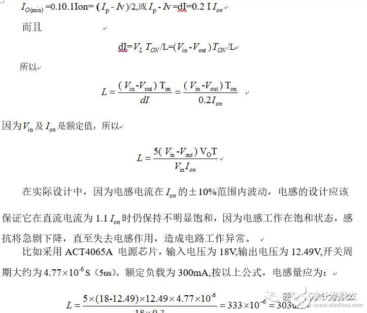
According to theoretical calculations, we should use 303uH, but in practice, we only use 68uH. Part of this is due to cost, and part is due to the physical constraints of the product itself, where space is limited and large inductors cannot be placed. Personally, I feel that 68uH is sufficient.
The following are some of the waveforms for the output load current threshold as a function of inductance when testing the ACT4065A:
1. L1=27uH, Uo=12.51V
By changing the magnitude of the load current and observing the output waveform, the oscillation waveform width decreases as the load current gradually increases at L1=27uH. When the waveform reaches 100mA, no waveform is generated when the waveform is turned off, and the normal switching state is reached.
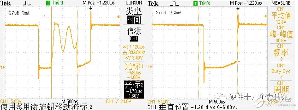
0mA 100mA
2. L1=33uH, Uo=12.51V
By changing the magnitude of the load current and observing the output waveform, the oscillation waveform width decreases as the load current gradually increases at L1=33uH. When the waveform reaches 55mA, no waveform is generated when the waveform is turned off, and the normal switching state is reached.
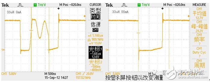
0mA 55mA
3. L1=47uH, Uo=12.51V
By changing the magnitude of the load current and observing the output waveform, the oscillation waveform width decreases as the load current gradually increases at L1=47uH. When the voltage reaches 45mA, no waveform is generated when the waveform is turned off, and the normal switching state is reached.
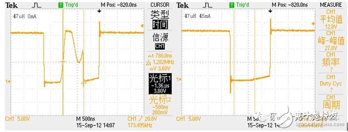
0mA 47mA
4. L1=68uH, Uo=12.51V
By varying the size of the load current and observing the output waveform, at L1=68uH, the oscillation waveform width decreases as the load current gradually increases. When the voltage reaches 30mA, no oscillation waveform is generated when the waveform is turned off, achieving a normal switching state.
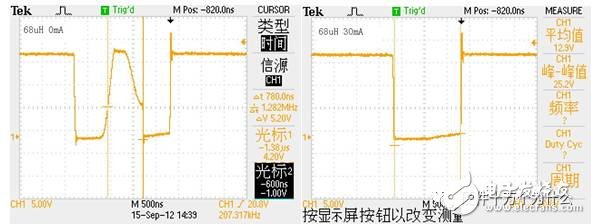
0mA 30mA
5. L1=136uH, Uo=12.51V
By changing the magnitude of the load current and observing the output waveform, at L1=136uH, the oscillation waveform width decreases as the load current gradually increases. When the voltage reaches 20mA, no waveform is generated when the waveform is turned off, and the normal switching state is reached.
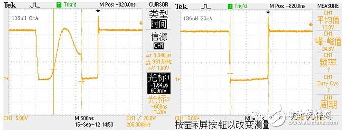
0mA 20mA
6. L1=204uH, Uo=12.51V
By changing the magnitude of the load current and observing the output waveform, at L1=204uH, the oscillation waveform width decreases as the load current gradually increases. When the voltage reaches 12mA, no waveform is generated when the waveform is turned off, and the normal switching state is reached.
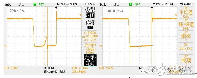
0mA 12mA
Based on the above and test waveforms, for the ACT4065A chip, when the inductance is gradually increased and the SW is turned off, the oscillation waveform width decreases; the larger the inductance, the smaller the load current needed to eliminate the oscillation waveform. However, this is only true within 10mA.
5. Comparison of CCM and DCM:
1. DCM is a great feature, it can reduce power consumption, and some DCM converters have higher efficiency, with full energy conversion;
2. Operating in DCM mode results in a larger output current ripple compared to CCM;
3. Operating in DCM mode causes oscillation when the inductor current reaches zero;
4. In CCM mode, the output voltage is independent of the load current. In DCM mode, the output voltage is affected by the load. To maintain a constant voltage, the duty cycle must change with the load current.
Some content is organized from Baidu Library.
Outdoor Fixed LED Display is a popular product for its high quality, every year sold to at least 80,000 pieces around the world, including Europe, North America, southeast Asia.Compared to other indoor LED display in the market, its biggest advantage is that it can display high-definition images while maintaining low power consumption.Besides, it adopts Die casting aluminum cabinet which is ultra-thin and ultra-light and owns good heat dissipation.Easy to install and maintain and suitable for multiple indoor scenes.
Application:
* Business Organizations:
Supermarket, large-scale shopping malls, star-rated hotels, travel agencies
* Financial Organizations:
Banks, insurance companies, post offices, hospital, schools
* Public Places:
Subway, airports, stations, parks, exhibition halls, stadiums, museums, commercial buildings, meeting rooms
* Entertainments:
Movie theaters, clubs, stages.
Outdoor Fixed LED Display,Led Wall Display Screen,Curved Led Display Screen,Led Display Board
Guangzhou Chengwen Photoelectric Technology co.,ltd , https://www.cwleddisplay.com