Working principle and application of 555 time base integrated circuit
The 555 time base circuit is a combined integrated circuit that combines analog functions and logic functions on the same silicon chip. It is novel in design, fantastic in design, and versatile. It is favored by electronic professional designers and electronic enthusiasts. People call it a great small IC. In 1972, Signetics developed the Tmer NE555 bipolar time base circuit, which was originally designed to replace mechanical retarders such as large thermal delay relays with poor timing accuracy. However, after the device was put on the market, it was found that the application of this circuit far exceeded the scope of use of the original design, and the application was widely used in various fields of electronic applications, and the demand was enormous. The major companies in the United States have imitated this circuit. In 1974, Sigridicx integrated two bipolar 555 units on the same substrate, named NF556. In 1978, Intel SIL Corporation (IntelSIL) Developed the CMOS type time base circuit ICM555 1CM556, and later introduced the four time base circuit 558 which integrates four time base circuits on one chip. 558 Due to the CMOS type process and high integration, the application of time base circuit is extended from civil to Rockets, missiles, satellites, aerospace and other high-tech fields. During this period, major companies and manufacturers in Japan and Western Europe competed for imitation and production. Although the world's major semiconductor or device companies and manufacturers are producing their own models of 555/556 time-base circuits, their internal circuits are similar and have the same lead-out function. The figure shows the internal equivalent circuit diagram of the CA555 time base circuit produced by American Radio Company.
Equivalent function circuit
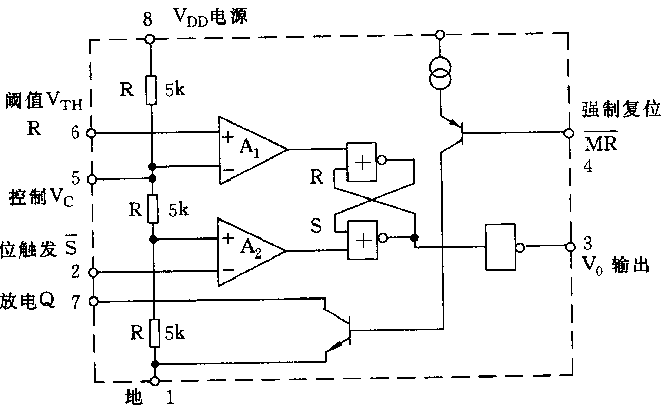
In view of the similar internal circuits of various bipolar 555 integrated blocks, we will use CA555 as an example to analyze its internal circuits and principles. From the internal equivalent circuit diagram of the CA555 time base circuit, it can be seen that VTl-VT4, VT5, VT7 constitute the comparator A1, and the base potential of VT7 is connected to the upper end of the voltage divider composed of three 5kΩ resistors, and the voltage is ? VDD; VT9-VT13 constitutes the comparator A2, the base of the VTl3 is connected to the lower end of the voltage divider, the reference potential is ? VDD. In circuit design, the three 5kΩ resistors that make up the voltage divider are required to have exactly the same resistance to give two more accurate reference potentials, VDD and VDD. VTl4-VTl7 is combined with a 4.7kΩ positive feedback resistor to form a bistable trigger circuit. The VTl8-VT21 forms a push-pull power output stage that can output approximately 200mA. VT8 is a reset amplifier stage, and VT6 is a discharge transistor that can withstand currents above 50mA. The operating state of the bistable trigger circuit is determined by the outputs of comparators A1, A2.
The working process of the 555 time base circuit is as follows: When the 2 pin, that is, the inverting input terminal of the comparator A2, is added with a trigger signal whose potential is lower than ?VDD, then VT9 and VT11 are turned on, and the VTl4 in the flip-flop is given. Provide a bias current, make VTl4 saturation conduction, its saturation voltage drop Vces clamps the base of VTl5 at a low level, makes VTl5 cut off, VTl7 is saturated, so that VTl8 is cut off, VTl9 is turned on, VT20 is fully saturated, VT21 cutoff . Therefore, the output 3 pin outputs a high level. At this time, regardless of the level of the 6-terminal (threshold voltage), due to the positive feedback of the 4.7kΩ resistor in the flip-flop (VTl4-VT17) (the base current of VTl5 is supplied through the resistor), The 3-pin output high state is maintained until the 6-pin appears above the VDD level. When the trigger signal disappears, that is, the potential of the inverting input terminal 2 of the comparator A2 is higher than ?VDD, then VT9 and VTll are turned off, and VTl4 is turned off due to no bias current. At this time, if the 6-pin has no trigger input, the Vces of the VTl7 is saturated. The voltage drop maintains the VTl3 cut-off through the 4.7kΩ resistor, so that the VTl7 saturation steady state does not change, so the output terminal 3 still maintains a high level. At the same time, the cutoff of VTl8 also cuts off VT6. When the trigger signal is applied to pin 6, and the potential is higher than ?VDD, then VTl, VT2, and VT3 are all turned on. At this time, if there is no external trigger signal on the 2 feet to turn off VT9 and VTl4, the collector current of VT3 is biased to VTl5, so that the stage is saturated, and VTl7 is turned off, and then VTl8 is turned on, VTl9, VT2. Both are off, VT21 is saturated, so the 3 pin outputs low level. When the trigger signal of the 6-pin disappears, that is, when the potential of the pin falls below VDD, VTl, VT2, and VT3 are all turned off, so that VTl5 cannot be biased. At this time, if there is no trigger signal on the 2 pin, VTl5 will get a bias current through the 4.7kΩ resistor, so that VTl5 maintains saturation conduction, and the steady state of VTl7 is cut off, so that the 3-pin output terminal is maintained at a low level. At the same time, the conduction of VTl8 makes the discharge stage VT6 saturate and conduct. Through the analysis of the above two states, it can be found that as long as the potential of the 2 pin is lower than ?VDD, when the trigger signal is added, the output pin 3 must be high; and when the potential of the 6 pin is higher than ?VDD When the trigger signal is added, and the potential of the 2 pin is higher than VDD, the output pin 3 has a low level output. 4 feet are the reset end. When a trigger signal is applied to the pin, that is, its potential is lower than the on-state saturation voltage drop of 0.3V, VT8 is turned on, and its emitter potential is lower than lV. Because D3 is connected, VTl7 is off state, VTl8, VT21 The saturation is turned on, and the output pin 3 is low. At this time, regardless of the potential of the 2nd and 6th feet, this state cannot be changed. Since the emitter of VT8 passes through the emitters of D3 and VTl7 to ground, the emitter potential of VT8 will not be higher than the 1.4V voltage under any circumstances. Therefore, when the potential of the reset terminal 4 is higher than 1.4V, the VT8 is in a reverse bias state and does not function, that is, the level of the output pin 3 at this time depends only on the potentials of the 2 pin and the 6 pin.
According to the above analysis, the internal equivalent circuit of the CA555 time base circuit can be simplified to the equivalent function circuit as shown. Obviously, the 555 circuit (or 556 circuit) contains two comparators A1 and A2, a flip-flop, a driver and a discharge transistor. The two comparators are set to ?VDD and ?VDD by voltage dividers composed of resistors R1, R2, and R3, respectively. The reference voltage is defined. In order to further understand its circuit functions and flexibly apply the 555 integrated block, the following is a brief description of its mechanism of action. As can be seen from Figure 1-5, a voltage divider consisting of three 5kΩ resistors causes the internal two comparators to form a level flip-flop with an upper trigger level of ?VDD and a lower trigger level of ?VDD. An external reference voltage Vc can be connected to the 5-pin control terminal to change the upper and lower trigger level values. The output of the comparator A1 is connected to the input of the NOR gate 1, and the output of the comparator A2 is connected to the input of the NOR gate 2. Since the RS flip-flop consisting of two NOR gates must be triggered by the negative polarity signal, the trigger signal applied to the 6-pin of the comparator A is only when the potential is higher than the potential of the inverting terminal 5, R - The S flip-flop is flipped; the trigger signal applied to the inverting pin 2 of the comparator A2 is only inverted when the potential is lower than the potential of the A2 non-inverting terminal, VDD.
Select Vape presents Bang xxl Switch DUO Disposable Device. Experience a mouthwatering sensation of two exquisite flavors packed in one disposable device wherever you go. The Bang XXL Switch DUO provides a 7ml (3.5ml/per flavor) juice capacity powered by an integrated 1100mAh non-rechargeable battery, delivering amazing flavor output. This device is operated via draw-activated firing mechanism and you can switch between flavors by using the switch located at the base. Each Bang XXL contains 6% nicotine and lasts roughly 2500~ puffs before disposal.
Designed for those who are always on the go, the Big Bang XXL Switch Duo Disposable Vape is an ultra-advanced vaping pod mod system that`s all about giving a rapidly smooth puff trip to all the meshuga vapers! This smart and compact mechanism of vaping will leave you with the perfect ` larger than life throat hits` without actually demanding anything. These pre-filled, pre-charged, vaping throwaways beat the rest for their unique blend of sleek designing yet giving vapers the double extra large puff feels!
To top it all is the flavor switching feature with an exquisite combination of tastes giving our taste buds an awesome flavor experience. The smart and sleek vape juice composition holds 6% of concentrated nicotine salt in the e-juice. The good news is that they are absolutely low maintenance! Slide your hand in the pocket and you are set for the extravagant 2500 flavor-rich,mess-free puffs!
FLAVOR PROFILE:
BANANA ICE/STRAWBERRY BANANA
COOL MINT/BLUEBERRY ICE
RED APPLE/GREEN APPLE
STRAWBERRY ICE/WATERMELON ICE
WATERMELON LUSH/BUBBLEGUM
STRAWBERRY APPLE WATERMELON/STRAWBERRY KIWI
BLUE RAZ/RED RAZ PASSION
VERY BERRY/GUMMY BEAR
disposable vape pen. bang xxl vape, vape disposable ,double flavor vape
Shenzhen Essenvape Technology Co., Ltd. , https://www.essenvape.com