Power MOSFET structure and working principle
Types of power MOSFETs: According to the conductive channel, it can be divided into P-channel and N-channel. According to the gate voltage amplitude, it can be divided into; depletion type; when the gate voltage is zero, there is a conductive channel between the drain and the source, and the enhancement type; for the N(P) channel device, the gate voltage is greater than (less than The conductive channel exists at zero time, and the power MOSFET is mainly N-channel enhancement type.
1. Structure of power MOSFET
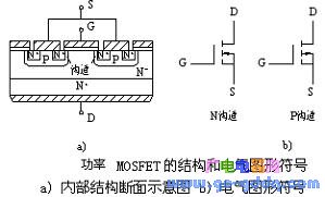
The internal structure and electrical symbol of the power MOSFET are shown in the figure above; when it is turned on, only one carrier (multi-sub) of one polarity participates in conduction, which is a unipolar transistor. The conductive mechanism is the same as that of the small power MOS tube, but the structure is quite different. The small power MOS tube is a lateral conductive device. The power MOSFET mostly adopts a vertical conductive structure, also known as a VMOSFET (VertICal MOSFET), which greatly improves the resistance of the MOSFET device. Pressure and current resistance.
According to the difference of vertical conductive structure, it is divided into VVMOSFET which realizes vertical conduction by V-groove and VDMOSFET (Vertical Double-diffused MOSFET) which has vertical conductive double-diffused MOS structure. This paper mainly discusses VDMOS device as an example.
The power MOSFET is a multi-integrated structure. For example, International Rectifier's HEXFET uses a hexagonal unit; Siemens' SIP MOSFET uses a square unit; Motorola's TMOS uses a rectangular unit. "Glyph arrangement.
2. The working principle of the power MOSFET
Cutoff: Positive power is applied between the drain and source, and the voltage between the gate and source is zero. The PN junction J1 formed between the P base region and the N drift region is reversely biased, and no current flows between the drain and the source.
Conductive: A positive voltage UGS is applied between the gate and source, and the gate is insulated, so no gate current flows. However, the positive voltage of the gate pushes the holes in the P region below it, and the minority electrons in the P region are attracted to the surface of the P region below the gate.
When UGS is greater than UT (on voltage or threshold voltage), the electron concentration on the surface of the P region under the gate will exceed the hole concentration, so that the P-type semiconductor is inverted into an N-type and becomes an inversion layer, and the inversion layer forms an N-channel. The PN junction J1 disappears and the drain and source are conducting.
3. Basic characteristics of power MOSFET
4. Static characteristics; its transfer characteristics and output characteristics are shown in the figure below.
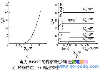
The relationship between the drain current ID and the gate-to-source voltage UGS is called the transfer characteristic of the MOSFET. When the ID is large, the relationship between ID and UGS is approximately linear, and the slope of the curve is defined as the transconductance Gfs.
The volt-ampere characteristics of the MOSFET (output characteristics): a cut-off region (corresponding to the GTR cut-off region); a saturation region (corresponding to the amplification region of the GTR); and an unsaturated region (corresponding to the saturation region of the GTR). The power MOSFET operates in a switching state, that is, switching back and forth between the cutoff region and the unsaturated region. There is a parasitic diode between the drain and source of the power MOSFET, and the device is turned on when a reverse voltage is applied between the drain and the source. The on-resistance of the power MOSFET has a positive temperature coefficient, which is advantageous for current sharing when the devices are connected in parallel.
5. Dynamic characteristics; the test circuit and switching process waveforms are shown below.
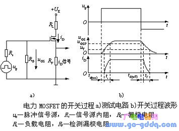
Turn-on process; turn-on delay time td(on) - the time period between the time when the front edge is up to uGS=UT and the iD starts to appear;
The rise time tr-uGS rises from uT to the time period during which the MOSFET enters the gate voltage UGSP of the unsaturated region;
The iD steady state value is determined by the drain supply voltage UE and the drain load resistance. The size of UGSP is related to the steady state value of iD. After UGS reaches UGSP, it continues to rise until it reaches steady state, but iD has not changed.
The turn-on time ton-the sum of the turn-on delay time and the rise time.
Shutdown delay time td(off) -up drops to zero, Cin discharges through Rs and RG, and uGS begins to decrease to zero when exponentially decreasing to UGSP.
The fall time tf-uGS continues to fall from UGSP, iD decreases, to the sum of the uGS turn-off time toff-off delay time and fall time.
6. Switching speed of the MOSFET.
The switching speed of MOSFET has a great relationship with Cin charge and discharge. Users can't reduce Cin, but it can reduce the internal resistance Rs of the drive circuit to reduce the time constant and speed up the switching speed. The MOSFET only depends on multiple sub-conductors, so there is no minority storage effect. The turn-off process is very fast, with switching times between 10-100ns and operating frequencies up to 100kHz, making it the highest of the major power electronics.
The field control device requires almost no input current when it is static. However, in the switching process, the input capacitor needs to be charged and discharged, and a certain driving power is still required. The higher the switching frequency, the greater the drive power required.
7. Dynamic performance improvement
In addition to considering the voltage, current, and frequency of the device, it must be known how to protect the device in the application without damaging the device in transient changes. Of course, the thyristor is a combination of two bipolar transistors, and the large capacitance due to the large area, so its dv/dt capability is relatively fragile. For di/dt, it also has an extension problem of the conduction area, so it also brings quite strict restrictions.
The situation of power MOSFETs is quite different. Its dv/dt and di/dt capabilities are often measured in terms of nanoseconds (rather than microseconds). But despite this, it also has dynamic performance limitations. These can be understood from the basic structure of the power MOSFET.
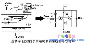
The figure below shows the structure of the power MOSFET and its corresponding equivalent circuit. In addition to the presence of capacitance in almost every part of the device, it must also be considered that the MOSFET is also connected in parallel with a diode. At the same time, from a certain point of view, it also has a parasitic transistor. (Like IGBTs also parasitize a thyristor). These aspects are important factors in studying the dynamic characteristics of MOSFETs.
First, the intrinsic diode attached to the MOSFET structure has a certain avalanche capability. It is usually expressed by a single avalanche ability and repeated avalanche ability. When the reverse di/dt is large, the diode will withstand a very fast pulse spike, which may enter the avalanche zone and may damage the device once it exceeds its avalanche capability. As a PN junction diode, careful study of its dynamic characteristics is quite complicated. They are very different from the simple concept that we generally understand that blocking is reversed when the PN junction is positive. When the current drops rapidly, the diode loses its reverse blocking capability in one stage, the so-called reverse recovery time. When the PN junction is required to be turned on quickly, there will be a period of time that does not show a very low resistance. In the power MOSFET, once the diode is forward implanted, the injected minority carriers also increase the complexity of the MOSFET as a multi-sub-device.
During the design of the power MOSFET, measures are taken to make the parasitic transistors therein as ineffective as possible. The measures are different in different generations of power MOSFETs, but the general principle is to make the lateral resistance RB under the drain as small as possible. The parasitic bipolar thyristor begins to fail because only the lateral resistance under the drain N region flows through a sufficient current to establish a positive bias for this N region. However, under severe dynamic conditions, the lateral current due to dv/dt through the corresponding capacitance may be sufficiently large. At this point, the parasitic bipolar transistor will start, which may damage the MOSFET. Therefore, attention must be paid to the individual capacitors inside the power MOSFET device (which is the channel of dv/dt) when considering transient performance.
Transient conditions are closely related to the condition of the line, and this aspect should be given sufficient attention in the application. A thorough understanding of the device will help to understand and analyze the corresponding problem.
12Inch Coaxial Speaker,12 Inch Coaxial,12 Inch Neodymium Coaxial Speaker,12 Inch Coaxial Speaker
Guangzhou BMY Electronic Limited company , https://www.bmy-speakers.com