Application of new MODEM chip CMX868
American Consumer Microcircuit Limited MX-COM Inc. The new CMX868 product developed by the company is a new multi-mode modem chip. Can be applied to low voltage V. The design of the 22bis modem. The function of the CMX868 chip has not been fully developed in China due to few related introductions. This article describes the design of a communication device using a microcontroller and the modem chip and its associated hardware. Because the performance requirements of the terminal are not very high (only need to send or receive data between 0 and 9999 to the outside world from time to time), it is constructed by a single-chip computer (such as AT89C51) whose price is less than one tenth of the PC. A terminal system that can control the behavior of the modem chip can meet the requirements, and can greatly reduce the operating cost of the device. 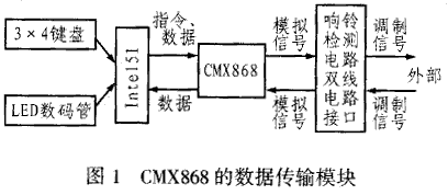
1 System working principle
1.1 CMX868 main chip
The CMX868 multimode modem is a low voltage V. The 22bis modem chip is ideal for embedded systems. It uses low-mesh CMOS technology, with a normal operating voltage of 2.7V, an operating current of 5A, and zero power consumption in the same state. CMX868 supports V. 22, Bell 212A? V. 23?Bell 202?V. Protocols such as 21, the maximum transmission rate is 2400bps. Setting its internal parameter register allows the chip to communicate with the outside world under a specific protocol. However, this setting will affect the way the signal is modulated and demodulated, and it also determines the signaling system used in the communication process.
1.2 Signal transmission
The transmission path of the CMX868 data signal in the system is shown in Figure 1. Among them, CMX868 and MCU are connected through the serial port, the chip is often in the "zero state" waiting mode, and the current consumption is only 1μA. The CMX868 in the zero state can be activated with the ring signal to put it into operation. The CMX868 chip can generate an interrupt signal IRQN to inform the microcontroller that it can receive the input data and then pass through the P1.0 pin of the microcontroller (connected to the CSN on the CMX868) and the T1 pin (connected to the SERIAL CLOCK on the CMX868). The CMX868 sends a signal. When they are in the "enable" state at the same time, the data and address can be transmitted through the two data lines COMAND DATA and REPLY DATA, respectively.
figure 2
In the past, the bell detection circuit and the two-wire interface circuit were usually connected to the CMX88 and the telephone line, respectively. 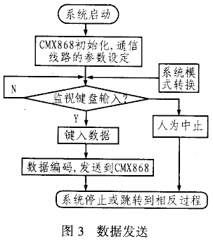 This design integrates the two into one, which simplifies the circuit and improves the reliability of the system.
2 hardware design
Figure 2 shows a CMX868-based Modem system circuit designed by the author. This circuit design refers to foreign related design principles and ideas [1]~[4], and also takes into account domestic factors such as component sources.
The design of the printed circuit board can be completed by the software protel99se, and the network table, layout and wiring can be imported after the principle design is completed, thereby completing the production of the printed circuit board.
3 software design
The main task of the system is to set the initialization of the CMX868 chip and the parameters of the communication line, and at the same time, the collected information is encoded and transmitted, and the received information is decoded and sent to the display system. The main program flow of the system can be divided into two relatively independent parts: “information transmission†and “information receptionâ€. Figure 3 and Figure 4 are respectively software flow diagrams for data transmission and reception of the system, and the program can be programmed in C language. Since the data receiving and transmitting process is constantly switched, when it is in "receiving information" 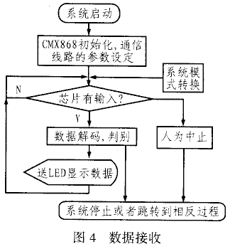 In the state, since the amount of data of the received information is not known, it may be necessary for the program to make a judgment on the received information, so that the mode conversion is performed after receiving the preset information. In addition, the initialization of the CMX868 and the parameter setting of the communication line are only necessary when the system is powered on, so it is not necessary to repeat during the mode conversion.
4 test results
The system is debugged between “Source†(System A) and “Sink†(System B). During commissioning, the circuit characteristics test and software and hardware joint debugging of the two systems are completed separately, and then the communication process between the two systems A and B is debugged. When the number 1234 is typed on the keyboard of system A, the data displayed by the system B digital tube is matched, thereby confirming that the developed system can meet the design requirements.
Wine Gifts ,Silicone Ice Tray,Wine Items ,Wine Glass Accessories
Hair Weaving & Hair Weft Co., Ltd. , http://www.nboutdoors.com