Third generation mobile phone RF architecture
Most telecom companies have invested heavily in getting 3G licenses, and now they need infrastructure investments to support this long-awaited technology. The total cost will be in the billions of pounds, so telecoms are under great pressure to repay their debts as quickly as possible and profit quickly. The fastest way to achieve this goal is to start the 3G consumer market as soon as possible.
For services such as price-competitive multimedia functions, the key to winning the favor of consumers and business customers and quickly recovering investment is to provide affordable mobile phones. The internal circuitry of the handset, including the transmitter and receiver, accounts for a significant portion of handset cost. To reduce the overall cost of 3G handset RF solutions, three main goals must be met: reducing chip cost, reducing external device requirements, and integrating as much external components as possible into a solution like a SoC. .
The standard range of wideband code division multiple access (W-CDMA) involved will become the main standard for 3G. However, in Europe, mobile phones also need to be able to support the existing GSM 900 and GSM 1800 standards. There is a similar situation in the US market, where high-end handsets still need to support the GSM 900 and GSM 1800 standards in a few years.
For RF designers who need to support the GSM Enhanced Data Rate Improvement (EDGE) standard, the problem is more complicated. EDGE will be used in suburban or rural areas to ensure that residents there can also enjoy the high data rate services provided by 3G, rather than limiting 3G to the major urban areas covered by W-CDMA. EDGE will complement W-CDMA and deliver data rates up to 384 kbps to a wider audience. The evolution process of 2G-3G is shown in Figure 1.
Integration in mobile phone design always has the requirement to further reduce the PCB board space. However, due to advances in technology in recent years, it has become easier in some respects to provide consumers with smaller and lighter mobile phones. For example, a lower power circuit means that a smaller battery can be used to achieve the same call and standby time.
The emergence of 3G brings new pressure to further reduce the size of the PCB. This requires the integration of larger multimedia displays and other features including cameras in 3G handset designs that are no larger than existing 2G models.
The pressure to reduce the overall cost of the phone is also high. From a circuit perspective, the best way to reduce costs is to integrate as many components as possible into the SoC solution with smaller geometries and lower cost processes. Integrating external components also brings additional benefits, including increased reliability, reduced production and assembly costs, and smaller EMC shielding issues.
Although it is possible to integrate multiple components in a single chip, isolation is required between the transmit and receive channels of W-CDMA in order to achieve duplexing, which is not feasible for GSM. Therefore, the 3G solution must also use two chips at this stage. Zarlink Semiconductor's transmit and receive chips are packaged in a microlead frame (MLF) surface mount package that requires only a small amount of space on a valuable PCB board. The transmitter chip has 40 pins and measures 6mm x 6mm, while the receiver chip has 56 pins and measures 8mm x 8mm. SiGe BiCMOS technology is used in the manufacturing process to achieve smaller geometry, lower cost, and lower power consumption. The structure used can eliminate expensive external components such as SAW filters. VCOs (including oscillator circuits), PLLs, LNAs, and HPA pre-driver circuits are also built in.
Receiver structure superheterodyne is a traditional and mature receive channel structure in radio transmission. However, this solution is not suitable for 3G applications because this architecture requires a large number of external components that are costly and take up a lot of PCB space.
Direct conversion is an optional architecture that can greatly reduce the number of external filters required. However, the direct conversion (zero intermediate frequency) structure also has disadvantages, and the control circuit becomes very complicated in order to compensate for the baseband DC offset. This compensation becomes more difficult for 3G RF units that need to support both EDGE and W-CDMA. This is because the control circuit must perform DC offset correction based on the amplitude modulation signal.
These problems have led to the need for a new 3G handset architecture that supports EDGE that can effectively meet the 3G application requirements in terms of cost and functionality. Near Zero Intermediate Frequency (NZIF) technology provides a compromise between superheterodyne and direct conversion techniques. In principle, it looks like a superheterodyne structure, but the difference is that it uses an intermediate frequency on a channel that is slightly higher than DC. By shifting the intermediate frequency to such a low frequency, it is possible to integrate the entire filtering function on a single chip. This means that there is no need to have an external IF SAW filter and DC bias control circuit operating at hundreds of MHz. For W-CDMA, the DC offset does not have much problem, and the DC component can be filtered out without greatly affecting the sensitivity. The only external filter required is the RF filter before the LNA.
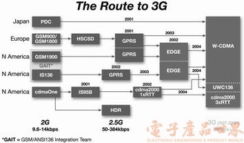
Figure 1 2G to 3G evolution process
The transmitter structure is on the transmit channel, and the "upconversion" architecture provides the simplest solution. However, due to the need for intermediate frequencies and expensive external filters, there are significant cost issues. Polar loops, offset PLLs, and direct modulation are all optional structures for 3G transmitters.
The bias PLL architecture has been widely used in GSM in recent years. This method removes all amplitude modulation (AM) components of the signal and provides a very clean spectrum. Unfortunately, this structure is not suitable for signals with AM content such as EDGE.
The polar loop technique is similar to the bias PLL, but allows the addition of an AM component to the RF signal. However, for W-CDMA, the application of this technique is also problematic because it is extremely difficult to achieve phase and amplitude synchronization, which is impossible in some cases.
It seems that the last technique, direct modulation, does not seem to work. Since the required local oscillator (LO) frequency needs to be the same as the transmitted signal, this can result in very large output signals resulting in VCO oscillator frequency pull problems. However, by doubling the LO frequency and then dividing the frequency, the LO will no longer operate at the same frequency as the transmitted signal, thereby avoiding the frequency pull problem. This structure is suitable for both W-CDMA and EDGE. This structure is also less expensive since no external components are required.
Current processes such as SiGe BiCMOS enable very clean, low noise VCOs. For W-CDMA, the VCO will operate above 4 GHz, at which it is possible to integrate all active components of the VCO, including the bias circuit and all the oscillating circuits. This means that the entire VCO can be integrated on the chip and then divided down to the required frequency band.
Conclusion The latest manufacturing processes and structural techniques can meet the key technical requirements of 3G handsets: the SiGe BiCMOS process allows both transmitter and receiver to maintain low power consumption while keeping physical dimensions as small as possible. The new system architecture design approach allows designers to reduce costs by eliminating external components or integrating them into the chip. In the future, in addition to further addressing the challenges, there is a need to find ways to integrate both transmitters and receivers on a fully integrated single chip. â–
For services such as price-competitive multimedia functions, the key to winning the favor of consumers and business customers and quickly recovering investment is to provide affordable mobile phones. The internal circuitry of the handset, including the transmitter and receiver, accounts for a significant portion of handset cost. To reduce the overall cost of 3G handset RF solutions, three main goals must be met: reducing chip cost, reducing external device requirements, and integrating as much external components as possible into a solution like a SoC. .
The standard range of wideband code division multiple access (W-CDMA) involved will become the main standard for 3G. However, in Europe, mobile phones also need to be able to support the existing GSM 900 and GSM 1800 standards. There is a similar situation in the US market, where high-end handsets still need to support the GSM 900 and GSM 1800 standards in a few years.
For RF designers who need to support the GSM Enhanced Data Rate Improvement (EDGE) standard, the problem is more complicated. EDGE will be used in suburban or rural areas to ensure that residents there can also enjoy the high data rate services provided by 3G, rather than limiting 3G to the major urban areas covered by W-CDMA. EDGE will complement W-CDMA and deliver data rates up to 384 kbps to a wider audience. The evolution process of 2G-3G is shown in Figure 1.
Integration in mobile phone design always has the requirement to further reduce the PCB board space. However, due to advances in technology in recent years, it has become easier in some respects to provide consumers with smaller and lighter mobile phones. For example, a lower power circuit means that a smaller battery can be used to achieve the same call and standby time.
The emergence of 3G brings new pressure to further reduce the size of the PCB. This requires the integration of larger multimedia displays and other features including cameras in 3G handset designs that are no larger than existing 2G models.
The pressure to reduce the overall cost of the phone is also high. From a circuit perspective, the best way to reduce costs is to integrate as many components as possible into the SoC solution with smaller geometries and lower cost processes. Integrating external components also brings additional benefits, including increased reliability, reduced production and assembly costs, and smaller EMC shielding issues.
Although it is possible to integrate multiple components in a single chip, isolation is required between the transmit and receive channels of W-CDMA in order to achieve duplexing, which is not feasible for GSM. Therefore, the 3G solution must also use two chips at this stage. Zarlink Semiconductor's transmit and receive chips are packaged in a microlead frame (MLF) surface mount package that requires only a small amount of space on a valuable PCB board. The transmitter chip has 40 pins and measures 6mm x 6mm, while the receiver chip has 56 pins and measures 8mm x 8mm. SiGe BiCMOS technology is used in the manufacturing process to achieve smaller geometry, lower cost, and lower power consumption. The structure used can eliminate expensive external components such as SAW filters. VCOs (including oscillator circuits), PLLs, LNAs, and HPA pre-driver circuits are also built in.
Receiver structure superheterodyne is a traditional and mature receive channel structure in radio transmission. However, this solution is not suitable for 3G applications because this architecture requires a large number of external components that are costly and take up a lot of PCB space.
Direct conversion is an optional architecture that can greatly reduce the number of external filters required. However, the direct conversion (zero intermediate frequency) structure also has disadvantages, and the control circuit becomes very complicated in order to compensate for the baseband DC offset. This compensation becomes more difficult for 3G RF units that need to support both EDGE and W-CDMA. This is because the control circuit must perform DC offset correction based on the amplitude modulation signal.
These problems have led to the need for a new 3G handset architecture that supports EDGE that can effectively meet the 3G application requirements in terms of cost and functionality. Near Zero Intermediate Frequency (NZIF) technology provides a compromise between superheterodyne and direct conversion techniques. In principle, it looks like a superheterodyne structure, but the difference is that it uses an intermediate frequency on a channel that is slightly higher than DC. By shifting the intermediate frequency to such a low frequency, it is possible to integrate the entire filtering function on a single chip. This means that there is no need to have an external IF SAW filter and DC bias control circuit operating at hundreds of MHz. For W-CDMA, the DC offset does not have much problem, and the DC component can be filtered out without greatly affecting the sensitivity. The only external filter required is the RF filter before the LNA.
Figure 1 2G to 3G evolution process
The transmitter structure is on the transmit channel, and the "upconversion" architecture provides the simplest solution. However, due to the need for intermediate frequencies and expensive external filters, there are significant cost issues. Polar loops, offset PLLs, and direct modulation are all optional structures for 3G transmitters.
The bias PLL architecture has been widely used in GSM in recent years. This method removes all amplitude modulation (AM) components of the signal and provides a very clean spectrum. Unfortunately, this structure is not suitable for signals with AM content such as EDGE.
The polar loop technique is similar to the bias PLL, but allows the addition of an AM component to the RF signal. However, for W-CDMA, the application of this technique is also problematic because it is extremely difficult to achieve phase and amplitude synchronization, which is impossible in some cases.
It seems that the last technique, direct modulation, does not seem to work. Since the required local oscillator (LO) frequency needs to be the same as the transmitted signal, this can result in very large output signals resulting in VCO oscillator frequency pull problems. However, by doubling the LO frequency and then dividing the frequency, the LO will no longer operate at the same frequency as the transmitted signal, thereby avoiding the frequency pull problem. This structure is suitable for both W-CDMA and EDGE. This structure is also less expensive since no external components are required.
Current processes such as SiGe BiCMOS enable very clean, low noise VCOs. For W-CDMA, the VCO will operate above 4 GHz, at which it is possible to integrate all active components of the VCO, including the bias circuit and all the oscillating circuits. This means that the entire VCO can be integrated on the chip and then divided down to the required frequency band.
Conclusion The latest manufacturing processes and structural techniques can meet the key technical requirements of 3G handsets: the SiGe BiCMOS process allows both transmitter and receiver to maintain low power consumption while keeping physical dimensions as small as possible. The new system architecture design approach allows designers to reduce costs by eliminating external components or integrating them into the chip. In the future, in addition to further addressing the challenges, there is a need to find ways to integrate both transmitters and receivers on a fully integrated single chip. â–
Triac Dimmable Constant Current LED Driver
Triac Dimmable Constant Current LED Driver,LED Driver Circuit,LED Controler,LED Transformer
LED Power Supply Co., Ltd. , http://www.nbleddriver.com