Design of Digital Video Signal Processing Circuit for LED Full Color Screen
The LED video display has high brightness, wide viewing angle, long life, high cost performance, and can display various texts, graphics, and images simultaneously with the computer. It can play video signals such as TV, video, and video discs in real time. Multimedia data and other advantages make it widely used in many public places such as streets, squares, commercial centers, sports venues, entertainment venues, and control centers. However, due to technical problems, the large video display still faces severe challenges, mainly manifested in low gray levels, severe loss of brightness, and low refresh rate. In addition, the video signal source in this article comes from the DVI (Digital Video Interface) interface. The DVI interface outputs digital video signals with a large amount of information. Generally, it is first buffered by an external RAM (Random Array Memory), and then the processor performs the video signal deal with. There are many types of external memory that can be used for digital image storage, such as SRAM, DRAM, and SDRAM, and their capacities and speeds vary. DRAM and SDRAM are dynamic memories with large capacity and need to be refreshed during use. When the processor does not have an external dynamic RAM interface, it is necessary to design a refresh circuit, which brings inconvenience to system applications; SRAM does not need to be refreshed, does not require a dedicated interface, real-time Good, and can jump addressing, so this article uses SRAM as an external cache memory. The use of sub-field partition storage technology greatly improves the refresh frequency, the image display effect is clear and stable, and realizes a video display system with a resolution of 800 × 256, a refresh frequency of 90 Hz, and 256 × 256 × 256 grayscale levels of red, green and blue . At the same time, with this technology, the brightness and gray level are easily adjustable and the brightness loss is small.
2 System composition
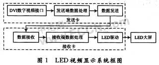
The overall block diagram of the LED video display system is shown in Figure 1: The system consists of two parts: sending and receiving. The function of the sending part is mainly to encode and decode the video signal transmitted by the DVI interface to form 24 b true color video data and dot clock (CLK ), Horizontal synchronization signal (HS), field synchronization signal (VS), data valid signal (DE) and other control signals are transmitted to the receiving card through LVDS (Low Voltage DifferenTIal Signaling) level, and then transmitted to With a specific driving structure (1/8 scanning mode, 74HC595 driving chip) rhythm LED large screen. The focus of this article is to introduce the data processing module of the receiving card.
3 Data processing
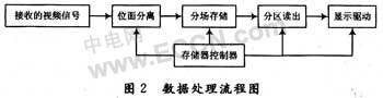
The data processing flow is shown in Figure 2: The receiving card receives the video signal (control signal and data signal) transmitted by the sending card, separates the data in the video signal through the bit plane, stores it in the external buffer in separate fields, and then reads out the partition, Transfer to the display driver screen. The bit-plane separation module reassembles the same weight bits of different data into new data and stores them in the memory. The external buffer adopts the technology of two SRAM ping-pong buffers to realize the pipeline processing of data. The principles and implementation of the bit-plane separation module and sub-field partition storage are introduced below.
3.1 Plane separation module
The gray scale control method adopted by the video display screen is a combination of sub-field superposition and duty cycle, as shown in Table 1: where sub-field superposition refers to the use of constant frequency scanning of different fields to achieve different gray levels, such as D7 ~ D4 of Table 1; Duty cycle control refers to controlling the duty cycle of the lighting time and the off time to realize the adjustment of gray scale, such as D3 ~ D0 of Table 1. The premise of these two methods is to achieve the separation of the video data plane. The bit-plane separation is realized by FPGA, which includes two major modules, a data shift register and a data selector. The principle block diagram realized by VHDL is shown in Fig. 3, where r0-7, g0-7 and b0-7 are the red, green and blue colors of the true color image data, each occupying one byte. Register these 24-bit data lines through an 8-bit wide data shift register, and then output them to an external buffer through a color bit selector. The bit-plane separation is realized by controlling the address of the buffer, and the data width of the external buffer is 24 bits, so that the RGB three colors are separated in parallel. Among them, the shift register uses pipeline technology, while latching the output of the same weight bits of the first 8 data, it shifts in the same weight bits of the 9th data, which improves the efficiency of data processing.

3.2 Split field storage
After the data is separated by the bit plane, the same weight bits of different data form new data. By controlling the address of the memory, the same weight bits of all data in a frame are written in the same segment of the memory, so the write address generator requires higher . The system requires 256 levels of gray, so the memory is divided into 8 segments, and each segment stores bits (fields) that represent the same weight. Among them, the 8 segments are replaced by 3 (23) address lines, the large screen with a resolution of 800 * 256 has 256 rows and 800 columns, then the row address is represented by 8 (28) address lines, and these 8 address lines The first 5 bits are the area address (32 areas), and the last 3 bits are the line address of one area (1/8 scan). The column address is represented by 7 (27) address lines. Because the memory is 24 bits wide, one storage unit represents the same weight bits of the 8 RGB points of the LED display, and the order of priority from high to bottom is: field address> column Address> line address. Implemented by counters respectively, the cascade of these three counters constitutes the write address of the memory, and the connection mode is: field address (A17 ~ A15), area address (A14 ~ A10), area line address (A9 ~ A7) Column address (A6 ~ A0). It can be seen that, by changing the priority of the memory address line, sub-field (8 field) storage can be realized.
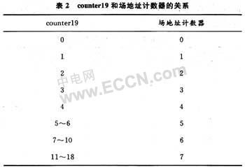
The data is written into the memory in 8 fields, and it needs to be read out in 19 fields when reading, and the display time of each field must be controlled. Therefore, when generating the field address counter of the read address, first design a 19-counter counter 19 (0 ~ 18). Table 2 shows the relationship between counter19 and the field address counter: the display time of each field is implemented with a comparator, and the grayscale and brightness can be flexibly corrected by changing the value in the comparator.
The LED display requires 32 zones to light up at the same time, and uses parallel processing of data to reduce hardware consumption and system operating frequency. Increase the refresh rate. Because the memory can only read one data at a time, it is necessary to use partition latching and then output the 32-area data in parallel.
Row address and column address have the same principle as the write address generator. Here we mainly introduce their priority. The data is already bit-plane separated, so if you want to display the 32 area data at the same time, then the priority of the area address should be the highest, followed by the column address, then the row address, and finally the field address. The connection with the memory is the same as the write address.
4 Simulation waveform
The simulation waveform of the bit-plane separation module is shown in Figure 4: RGBdin [23..16] is the upper eight bits of the input data, and rgb_regroup_output [23..16] is the upper eight bits of the output data. flag is a valid signal flag for input data, and flag_delay85 is a flag for valid signal output.
The waveform analysis is as follows:
The first 7 of the first 8 data of the input data are all 00h, and the 8th is 02h. After the 8 data are separated by the bit plane, the output is shown in Table 3. From Table 3, it can be seen that the first 8 data conversion is realized by the bit plane separation. Read from right to left after setting.
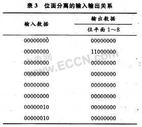
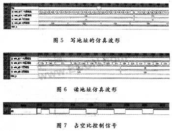
Figure 5 is the simulation waveform of the write address. It can be seen that the field address has the highest priority. When the field address is 7h, the column address is increased by 1. When the column address is 63h, the row address is increased by 1. When the row address is 7h, the zone address plus 1. For the same reason, it can be seen that the carry order of the read address in Figure 6 is: when the zone address is 1Fh, the column address is increased by 1, when the column address is 63h, the row address is increased by 1, and when the row address is 7h, the field address is counted according to the 19 field principle . When the line address in Figure 6 is 7h, the field address is not incremented. Fig. 7 is the duty signal controlled by the field address counter. This signal is connected to the enable end of the line drawing signal of the display driver board, and the display time is controlled by controlling the scanning signal, thereby realizing the gray level.
5 Conclusion
Aiming at the refresh speed and gray scale control problems encountered by the LED video display system, this paper proposes a sub-field partition storage technology, and introduces its principles and implementation in detail. Through waveform simulation and engineering application, this method solves the problem of image flicker and large brightness loss in the LED display control system, and its gray scale and brightness control can be flexibly corrected.
As one of the Oil Filled Transformers manufacturers, FGI`s S11 S13 series oil filled transformers have superior performance and remarkable energy-saving effect, reaching the international advanced level. The Oil Filled Transformer has the advantages of no lifting core, free maintenance, easy installation and low operating cost. The coil has low temperature rise, strong overload capability, and the body has a firm structure and strong short-circuit resistance.
Oil Filled Transformers
Oil Filled Transformer,Oil Filled Distribution Transformers,Oil Immersed Transformer,Oil Immersed Distribution Transformer,Liquid Filled Transformers,Oil Immersed Power Transformer
FGI SCIENCE AND TECHNOLOGY CO., LTD , https://www.fgi-tech.com