DS2141A, DS2143, DS2151, DS215
Abstract: This applicaTIon note contains informaTIon necessary to interface a nonmulTIplexed bus processor to the following Dallas Semiconductor T1 or E1 framers and single chip transceivers (SCTs): DS2141A, DS2143, DS2151, or the DS2153. These devices were originally designed to interface with a processor that uses a mulTIplexed bus configuration. With some additional external logic and minor changes to the software, any nonmultiplexed processor can be connected to these devices. The obvious benefit to the designer is the wider range of processor which will be able to interface with these devices. The application note contains a diagram which illustrates how to connect the multiplexed address and data bus to the processors independent address and data bus. It contains the necessary Dallas Semiconductor bus timing diagrams. Finally, it has information on how to write software which will allow the bus interface to read and write to the Dallas Semiconductor devices. The goal is to give t he designer all the information necessary to get the hardware and software communicating with the device.
The DS2141A, DS2143, DS2151 and DS2153 contain some internal circuitry to allow them to more easily interface to an external controller that has a non-multiplexed address / data bus. In multiplexed schemes like the DS2141A, DS2143, DS2151 and DS2153 uses, a signal exists (usually called Address Strobe or Address Latch Enable) to denote that a valid address is present on the bus. This signal is necessary because the address and data lines share the same bus. In non-multiplexed schemes, this signal may not be supplied by the controller because the address and data lines are separated. The DS2141A, DS2143, DS2151 and DS2153 contains some onboard circuitry that enables it to internally create an address latch if it is used on a non-multiplexed bus.
The creation of this internal address latch occurs as follows. In the Intel timing set, when the ALE pin on the DS2141A, DS2143, DS2151 and DS2153 is high, if the WR pin goes active (ie, low), then the address will be latched on the rising edge of WR. In the Motorola timing set, when the AS pin is high and the R / W pin is low, if the DS pin goes active (ie, high), then the address will be latched on the falling edge of DS.
As an example, in a non-multiplexed system, A0 could be tied to the ALE (or AS) input. Please see Figure 1. Each read or write to the DS2141A, DS2143, DS2151 and DS2153 would consist of two operations. To write to the DS2141A, DS2143, DS2151 and DS2153, first the controller would write the address and then the data. To read from the DS2141A, DS2143, DS2151 and DS2153, the controller would first write the address and then read the data. The addresses would be treated as data by the controller. The addresses would reside in odd numbered bytes while the data would reside in even numbered bytes. Please see Figures 2 through 4 for timing information. The parametrics listed in the DS2141A, DS2143, DS2151 and DS2153 data sheets are valid for non-multiplexed bus operation as well.
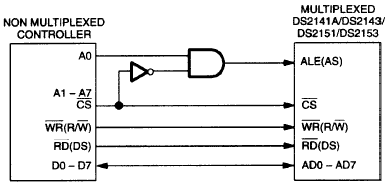
Figure 1. Non-multiplexed bus configuration.
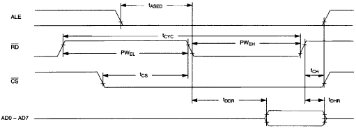
Figure 2. Non-multiplexed intel read timing.
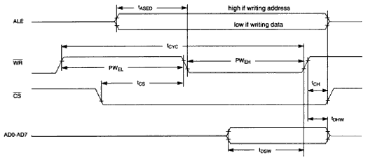
Figure 3. Non-multiplexed intel write timing.
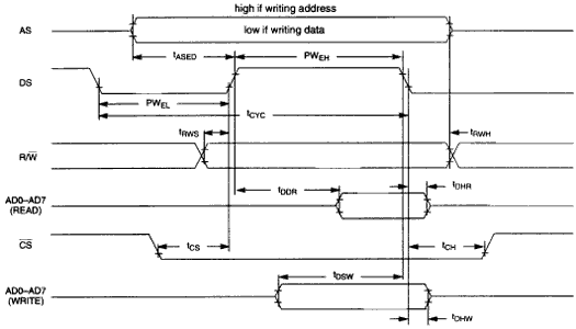
Figure 4. Non-multiplexed motorola timing.
The DS2141A, DS2143, DS2151 and DS2153 contain some internal circuitry to allow them to more easily interface to an external controller that has a non-multiplexed address / data bus. In multiplexed schemes like the DS2141A, DS2143, DS2151 and DS2153 uses, a signal exists (usually called Address Strobe or Address Latch Enable) to denote that a valid address is present on the bus. This signal is necessary because the address and data lines share the same bus. In non-multiplexed schemes, this signal may not be supplied by the controller because the address and data lines are separated. The DS2141A, DS2143, DS2151 and DS2153 contains some onboard circuitry that enables it to internally create an address latch if it is used on a non-multiplexed bus.
The creation of this internal address latch occurs as follows. In the Intel timing set, when the ALE pin on the DS2141A, DS2143, DS2151 and DS2153 is high, if the WR pin goes active (ie, low), then the address will be latched on the rising edge of WR. In the Motorola timing set, when the AS pin is high and the R / W pin is low, if the DS pin goes active (ie, high), then the address will be latched on the falling edge of DS.
As an example, in a non-multiplexed system, A0 could be tied to the ALE (or AS) input. Please see Figure 1. Each read or write to the DS2141A, DS2143, DS2151 and DS2153 would consist of two operations. To write to the DS2141A, DS2143, DS2151 and DS2153, first the controller would write the address and then the data. To read from the DS2141A, DS2143, DS2151 and DS2153, the controller would first write the address and then read the data. The addresses would be treated as data by the controller. The addresses would reside in odd numbered bytes while the data would reside in even numbered bytes. Please see Figures 2 through 4 for timing information. The parametrics listed in the DS2141A, DS2143, DS2151 and DS2153 data sheets are valid for non-multiplexed bus operation as well.
Figure 1. Non-multiplexed bus configuration.
Figure 2. Non-multiplexed intel read timing.
Figure 3. Non-multiplexed intel write timing.
Figure 4. Non-multiplexed motorola timing.
Nickel Iron Battery,Nickel Iron Alkaline Battery,Solar Battery,Nickel Iron Battery For Solar
Henan Xintaihang Power Source Co.,Ltd , https://www.taihangbattery.com