Three-phase power using Modbus protocol is built by 16-bit MSP430 processor
With the development of electric power automation technology and the need for the construction of electric power intelligent distribution systems, digital, intelligent, networked, and multi-functional distribution systems are becoming the most basic requirements for low- and medium-voltage distribution, using dedicated three-phase electrical parameters The intelligent power distribution system constructed by the acquisition chip and the cost-effective 16-bit MSP430 processor, and the universal Modbus protocol of the power system are realized through the RS 485 bus. Good sex and other advantages.
1 Hardware design of three-phase power distribution system
1.1 TI MSP430F149 processor
TI MSP430F149 is an ultra-low-power, cost-effective reduced instruction set 16-bit microcontroller, minimum instruction cycle 125 ns, 32 kB FLASH and 2 kB RAM, with rich on-chip peripheral resources and 5 bidirectional 8-bit IO ports, And has JTAG debugging interface, very suitable for the design of cost-effective low-power systems.
1.2 SA9904B three-phase electrical parameter acquisition chip
SA9904B of SAMES company is a special electrical parameter acquisition and measurement chip. This chip has real-time measurement of three-phase active and reactive power / energy, voltage effective value and line frequency, and can calculate power factor, current effective value and other parameters; The precise reference voltage guarantees the accurate collection of all electrical parameters; it has an SPI bus to facilitate interface with the processor; the chip itself consumes less than 60 mW and has ESD protection.
1.2.1 Internal structure and function of SA9904B
SA9904B is a high-precision dedicated electrical energy measurement chip, suitable for three-phase three-wire and three-phase four-wire, the internal structure shown in Figure 1. Internally integrated six-channel second-order 24-bit sigma-delta analog-to-digital converter, reference voltage circuit and digital signal processing circuit for active and reactive energy, effective value, main frequency measurement, can measure and calculate the active power of each phase, Important electrical parameters such as reactive power, active energy, reactive energy, voltage effective value, current effective value, power factor and frequency, etc. SA9904B provides a standard SPI bus interface to facilitate the transfer of electrical parameters with external processors.

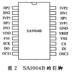
1.2.2 SA9904B pins and functions
The pin of SA9904B is shown as in Fig. 2. Where GND is the analog ground; VDD is the positive pole of the power supply, when using the shunt resistor to detect the current, connect to +2.5 V voltage; when using the current transformer, connect to +5 V voltage; VSS is the negative pole of the power supply, when using the shunt resistor When detecting current, connect a 2.5 V voltage, when using current transformer, connect 0 V voltage; IVPl, IVP2, IVP3 are three-phase analog voltage sampling input terminal, when the measured voltage is rated voltage, to ensure The effective value of the current input to the internal A / D converter is 14μA; IIPl, IINl, IIP2, IIN2, IIP3, and IIN3 are the three-phase analog current sampling input terminals. When the measured current is the rated current, ensure that the input to The current effective value of the A / D converter on the chip is 16μA; VREF is the external resistance end of the reference power supply, usually need to connect a 47 kΩ resistor to ground; F50 is the voltage zero-crossing pulse output end, and the output pulse frequency is AC Frequency, pulse width is 1 ms; CS, DI, DO, SCK are chip select end, data input end, data output end and clock end of SPI interface; OSCl, OSC2 are input and output ends of external crystal oscillator.
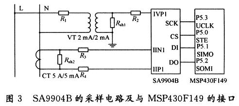
1.2.3 Sampling circuit of SA9904B and interface design with MSP430F149
The sampling circuit of SA9904B is divided into three-phase voltage and three-phase current sampling circuits. The sampling circuit generally has two forms of direct resistance voltage divider network sampling and mutual inductor sampling. The resistance voltage divider network sampling cost is low and the circuit is simple, but the sampling system is directly connected. There is no isolation into the power grid, and it is susceptible to impulse interference from the power grid. In severe cases, it will damage the system. This method is generally not used in industrial sites. The other is the voltage transformer and current transformer sampling circuit, which can effectively isolate the interference of the power grid to the system, ensure the accuracy of sampling and protect the measurement and control system. In this design, the sampling uses voltage transformer and current transformer sampling circuits. Figure 3 shows the voltage and current sampling of a one-phase circuit, and the other two-phase sampling circuits are the same. For the voltage sampling circuit, the selected voltage transformer is a current-type voltage transformer, the typical value is 2 mA / 2 mA, R1 is the front-end current limiting resistor, Rsh1 is the terminal resistance of the voltage transformer, R2 is the current limiting resistor of voltage sampling And, it must be satisfied that when the measured voltage is the rated voltage, the effective current value of the input IVPl is 14μA. If the rated voltage is 220 V, then R1 = If R2 selects 1 MΩ, then Rsh1 = 14 kΩ. For the current sampling circuit, the differential sampling input can be used to effectively suppress interference. The typical value of the selected current transformer is 5 A / 5 mA, Rsh2 is the terminal resistance of the current transformer, R3 and R4 are the current limiting resistors for current sampling, To satisfy that when the measured current is the rated current, the effective current value of the input current channels IINl and IIPl is 16 μA. If the rated current of the line to be measured is 5 A and R3 and R4 are equal, then ![]() If R3 = R4 = 100 kΩ is selected, then Rsh2 = 320Ω is obtained.
If R3 = R4 = 100 kΩ is selected, then Rsh2 = 320Ω is obtained.
MSP430F149's UARTl can be directly connected to SA9904B's SPI bus using SPI mode. MSP430F149 internally generates standard SPI timing. It uses 4-wire master-slave communication mode. MSP430F149 works in host mode. STE is the SPI gate control terminal. The UCLK signal is the synchronous clock of the SPI bus. In the first UCLK cycle, the data that has been written to UTXBUF is moved into the shift register in the order of high bit first and low bit behind, and it is shifted out by the SIMO pin and latched from the SOMI pin The data is sent to the receive shift register. When the receive shift register is full, the access data is placed in the receive buffer URXBUF. The first data bit received in the receiving process is the high bit. At this time, the URXIFG bit is set and the interrupt can be used. Or query the way to read the received data to complete a communication process. The SPI bus interface mode is shown in Figure 3.
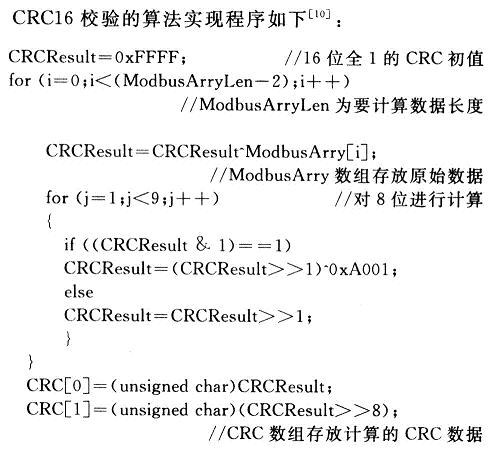
2. 2 Modbus RTU protocol communication realization
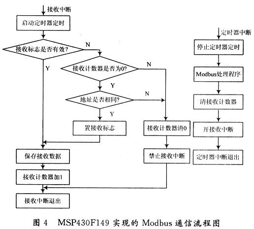
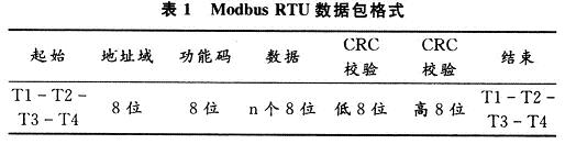
Modbus RTU mode programming must deal with the start and end time interval of the data packet, that is, the time interval of at least 3.5 characters between the two data packets, in order to ensure the integrity of the received data packet, when the receiver detects When a data packet starts, it starts to receive data, and compares the first data received, that is, the address field, with its own address. If it is the same, it receives the complete data packet and does a CRC check. If the addresses are different, the receiving process is abandoned and the start of the next data packet is awaited. When implemented in MSP430, a timer interrupt is used to detect the data interval between data packets, and the implemented program flow is shown in Figure 4.
The designed three-phase power intelligent power distribution system based on Modbus communication protocol, the software and hardware involved have been debugged, work normally and have stable performance. The module can be used alone as a three-phase power distribution module, and can also be easily connected to the Modbus communication network to achieve compatibility with other Modbus devices, and can be widely used in low-voltage power distribution systems.
The copper base board is the most expensive one among the metal substrates, and the heat conduction effect is many times better than that of the aluminum substrate and the iron substrate. It is suitable for high-frequency circuits and regions with high and low temperature variations and the heat dissipation and architectural decoration industries of precision communication equipment.
Generally, the finishing include ENIG, immersion silver, LF HASL, OSP, etc. The copper substrate circuit layer is required to have a large current carrying capacity, so a thick copper foil should be used, and the thickness is generally 35 μm to 280 μm; the thermal conductive insulating layer is the core technology of the copper substrate, and the core thermal conductive component is aluminum oxide and silicon powder. It consists of a polymer filled with epoxy resin, low thermal resistance (0.15), excellent viscoelasticity, resistance to heat aging, and ability to withstand mechanical and thermal stresses.
Copper Base Pcb,Copper Circuit Board,Heavy Copper Pcb,Copper Clad Pcb
Chuangying Electronics Co.,Ltd , https://www.cwpcb.com