Three minutes brings you in-depth understanding, operation and implementation of diode-based integrated RF detector interface
Figure 1 shows a widely used diode-based RF detection circuit schematic. Think of it as a simple half-wave rectifier with output filtering. The positive half cycle of the input signal forward biases the Schottky diode, which in turn charges the capacitor. During the negative half-cycle, the diode is reverse biased, causing the voltage on the capacitor to stay on, producing a DC output that is proportional to the input signal. In order to let this voltage drop when the input signal goes down or shuts off, a parallel combination of resistor and capacitor is used to provide the discharge path.
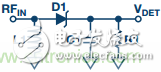
Figure 1. Diode-based Schottky RF detector
Figure 2 shows the transfer function of this circuit. The input power is adjusted in dB and the output voltage is represented by a logarithmic vertical scale. Observe the 25°C transfer function and find that there are two different working ranges on the curve. The area called the linear interval is the top of the input range (about 15 dBm) to about 0 dBm. The term "linear interval" is derived from the fact that the output voltage in this area is roughly proportional to the input voltage.
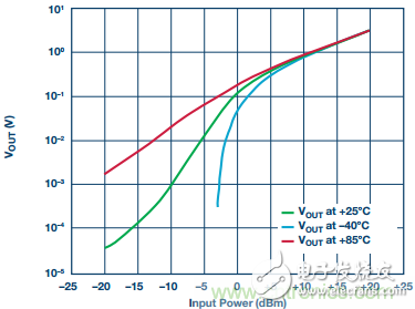
Figure 2. Diode-based Schottky RF detector transfer function
Below 0 dBm is the so-called square law area. In this area, the output voltage is roughly proportional to the square of the input voltage. This leads to a higher slope of the curve.
Figure 2 also shows the relationship between the circuit output voltage and the input power transfer function at –40°C and +85°C. It shows that the power level deviation below 0 dBm is large. This makes the device unstable in applications where the temperature changes slightly.
There are some techniques that can mitigate temperature drift to some extent. These techniques include the introduction of a second reference diode as part of the circuit, or as a stand-alone circuit with independent outputs. The reference diode temperature drift matches the main diode. By subtraction processing (analog domain or digital domain, depending on the circuit configuration), drift can be eliminated to a certain degree.
Figure 3 shows the ADL6010, a diode-based integrated Schottky detector with a number of innovative features—a transfer function at 25 GHz. As part of the signal processing, the input signal passes through a circuit that performs a square root operation only when the signal is below a certain power level. The transition point is intentionally set equal to the power level at which the diode transitions from the square law interval to the linear interval. Therefore, the square-law effect of the diode is eliminated, and the transfer function of the two intervals is not as obvious as in FIG.
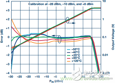
Figure 3. Relationship between output voltage and input power and linearity error of integrated Schottky diode detector at 25 GHz
Figure 3 also shows the transfer function curves for various temperatures ranging from –55°C to +125°C. In addition, the transfer function changes with temperature. Using the linear regression of the 25°C transfer function as a benchmark, the error at each temperature is plotted in dB. Due to the integrated temperature compensation circuit and the square-law cancellation circuit, it can be seen that the error caused by the linearity and temperature drift is about ±0.5 dB over most of the input range.
ADC interfaceAlthough RF and microwave detectors 1 are sometimes used in analog power control loops, it is more common to build a digital power control loop, as shown in Figure 4. In these applications, the output of the power detector is digitally processed using an analog-to-digital converter. In the digital domain, the power level is calculated using the code from the ADC. Once the power level is obtained, the system responds by adjusting the transmission power as needed.
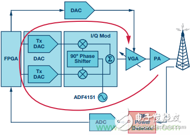
Figure 4. Typical CNC RF Power Control Loop
Although the response time of this loop only depends to a lesser extent on the detector response time, the ADC sampling rate and the speed of the power control algorithm will have a much greater impact.
The ability to measure the loop and precisely set the RF power level is affected by a number of factors, including the RF detector's transfer function and ADC resolution. To better understand this, let us take a closer look at the response of the detector. Figure 5 compares the response of the diode-based detector ADL6010 at 20 GHz to the microwave logarithmic amplifier HMC1094. Logarithmic amplifiers have a linear-in-dB transfer function, and a 1 dB change in input power always results in the same voltage change at the output (approximately –50 dBm to 0 dBm linear input range). In contrast, diode-based detectors, such as the ADL6010, have an exponential transfer function where the horizontal axis is measured in dB and the linear vertical axis is used for the output voltage.
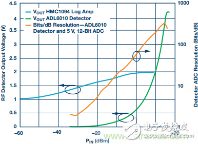
Figure 5. Linear dB comparison
Since the ADC's transfer function units are bits/voltages, this means that the system resolution expressed in dB/bit will continue to decrease as the input power decreases. The plot in Figure 5 also shows the bit/dB resolution that can be achieved with the ADL6010 driving a 12-bit ADC at 5 V full-scale voltage (for ease of viewing, the plot is scaled with the logarithmic counter axis). At about -25 dBm at the low end of the device's power range, the incremental slope is about 2 bits per dB, giving a resolution of about 0.5 dB/bit. This means that a 12-bit ADC is sufficient to accurately resolve the ADL6010 output at full scale.
As the RF input power increases, the increasing slope in bits/dB will steadily increase to a maximum of about 300 bits/dB at the maximum input power of 15 dBm. This is valuable for RF power control applications; the precision performance of such applications is critical when the system reaches maximum power. The RF detector is a very typical application scenario for measuring and controlling high power amplifiers (HPAs). In applications where it is often necessary to control power to prevent HPA from overheating, high resolution power measurements at maximum power are of great value.
In contrast, the HMC1094 logarithmic amplifier transfer function in Figure 5 also shows that its slope is constant over the linear operating range. This means that to achieve a resolution well below 1 dB, it is sufficient to use a lower resolution ADC (10 bits or even 8 bits).
In the application circuit shown in Figure 6, the ADL6010 interfaces with the AD7091, which is a 12-bit precision ADC with a sampling rate of up to 1 MSPS. The ADC has a built-in 2.5 V reference that sets the full-scale input voltage. Since the maximum voltage achievable with the ADL6010 detector is approximately 4.25 V, a simple resistor divider can be used to adjust the voltage down so that it never exceeds 2.5 V. This adjustment can be done without an op amp buffer. The achievable dB/bit resolution at the lower limit of the input power range is similar to the previous example (ie, approximately 0.5 dB/bit). 2
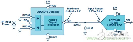
Figure 6. Integrated Microwave Power Detector and Precision ADC Interface
in conclusionIntegrated RF and microwave detectors offer many advantages over discrete deployments. The integrated temperature compensation circuit provides ready-to-use output voltage, which can be stabilized within ±0.5 dB over a wide temperature range. Using the internal square root function can effectively eliminate the square law characteristic at low input power levels. This allows a single linear transfer function to make device calibration easier. The buffered output of the integrated detector can directly drive the ADC without worrying about the load affecting the calculation accuracy. Care must be taken when selecting and designing an ADC to have enough bits/dB at low input power.
16+ Years Experience Smart Watch manufacturer, ITOPNOO Provide One-stop Smart Wearable devices Solutions For You.
Our Smart Wearable products include android smart watches, Watch For iPhone, Bracelet and Wristband etc.
Leading healthcare navigation services for individuals and families who are generally healthy or face serious medical issues, and health services for employers.
The Trends New Watches Designs. Custom smart watch products designed with the vision of our clients' brands in mind.
Wholesale smart watches,Best Smart Watches,Gifts Wholesalers, smart watch manufacturer
TOPNOTCH INTERNATIONAL GROUP LIMITED , https://www.micbluetooth.com