High-precision multi-function electronic clock based on 52 single-chip microcomputer and DS12C887
DS12C887 clock chip can automatically display year, month, day, hour, minute, second and other time information, but also has school hours, timekeeping, alarm clock and other functions. DS12C887 can also easily be adjusted or increased by software programming. Therefore, the design of a high-precision clock based on the DS12C877 clock chip has very important practical significance and practical value.
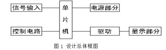
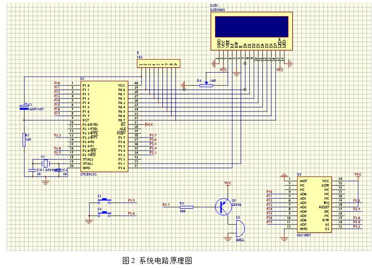
DesignBased on the traditional microcontroller-based digital clock design, after some improvements, the introduction of DS12C887 time chip, this design can be divided into two parts: the hardware part includes: small volume-rich STC89C52 microcontroller, with power-down protection DS12C887 clock chip The circuit is simple and easy to implement 1602LCD liquid crystal display, keyboard input circuit and so on. Specifically speaking, the system intelligent control part consists of a single-chip microcomputer and its related peripheral circuits. The peripheral circuits include a reset circuit for solving problems such as crashes, a stable-waveform crystal oscillator circuit, a keyboard design, an alarm circuit, and a suitable DC power supply circuit.
The use of a microcontroller to reset the circuit, reduce the power consumption and reduce the display external circuit display circuit, power supply circuit, etc. correctly connected together, and through the programming of the microcontroller to achieve the requirements of this design task. The software part mainly includes the main program module, DS12C887 module, LCD1602 module, keyboard control module. The DS12C887 chip has a brown-out protection function. It has a built-in lithium battery and can hold time information in the event of a power failure. It is not necessary to adjust the time after the external circuit is restored to power. This saves a lot of time for clock timing operation. The design is more energy-efficient, and the main circuit can be energized during the day, such as during daylight hours. It is possible to power off the main circuit without observing the clock at night, which saves a lot of power.
The time chip DS12C887 uses an internal integrated crystal oscillator circuit and has an internal temperature drift compensation circuit design. Accurate timing and accurate time are provided, which simplifies the device selection of the circuit, and also makes the program design more concise. In terms of hardware design, since only one DS12C887 time chip is added, it is not particularly complicated, and this independent timing design makes product troubleshooting more convenient.
Detailed design processFirst, system composition
1, system principle and hardware design
The design topic of this time is the design of the electronic calendar. It is required to realize the normal display of year, month, day, hour, minute, and second, which requires the combination of hardware and software. This design uses the features of the clock calendar chip DS12C887 and the functional use of the STC89C52 microcontroller. According to the requirements of the design, the calendar displays the year, month, day, hour, minute and second as the LCD1602.
After clarifying this design idea, draw a design block diagram. The overall block diagram is shown in Figure 2.1.
2, hardware selection
(1) The clock chip selects DS12C887 clock chip.
(2) The choice of the one-chip computer chooses STC89C52 one-chip computer, and it is equipped with 11.0592MHz crystal, the reset circuit adopts power-on reset.
(3) The display circuit selection uses LCD1602 liquid crystal display.
(4) The power supply is powered by a DC 5V power supply.
3, single-chip STC89C52 Chinese data
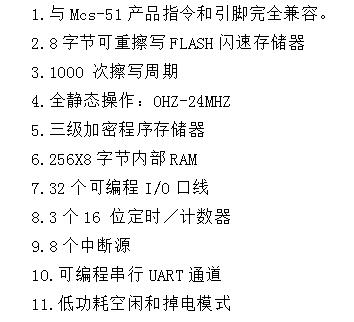
STC89C52 is a low voltage, high performance CMOS 8-bit microcontroller manufactured by STC. The chip contains 8K byTES re-erasable read-only program memory (PEROM) and 256 bytes of random access data memory (RAM). The device is manufactured using STC's high-density, non-volatile memory technology, and the standard MCS. The -51 instruction system and the 8052 product are pin compatible. The on-chip general-purpose 8-bit CPU and FLASH are memory cells. The STC89C52 is a one-chip powerful device that is suitable for many electronic products.
The main performance parameters:
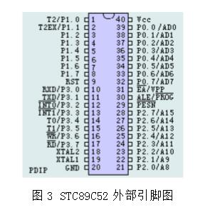
Vcc: Supply voltage GND: Ground
P0: The P0 port is a group of 8-bit open-drain bidirectional 1/O ports, which is also the address/data bus multiplexed port. When used as an output port. Each bit can sink 8 currents to drive 8 TTL logic gates. Writing “1†to port P0 can be used as a high impedance input.
When accessing external data memory or program memory, this group of line-time-time-sharing conversion addresses (low 8 bits) is multiplexed with the data bus, activating an internal pull-up Resistor during access.
When FLASH is programmed, port P0 receives the command byte, and when the program is verified, the command byte is output. When verifying, an external pull-up resistor is required.
Port P1: The PI is an 8-bit bidirectional I/O port with an internal pull-up resistor. The P1 output buffer stage can drive (absorb or output current) four TTL logic gates. Write “1†to the port and pull the port high through the internal pull-up resistor, which can be used as an input port. When used as an input port, a current IIL is output when a pin is pulled low by an external signal because of an internal pull-up resistor.
The difference from AT89C51 is that Pl.0 and P1.1 can also be used as the external count input (Pl.0/T2) and input (P1.1/T2EX) of Timer/Event Counter 2 respectively. See Figure 3
During FLASH programming and program verification, P1 receives the lower 8-bit address.
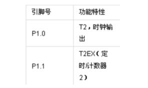
Fig. 3 The second function of PI.O and PI.l
Port: P2 is an 8-bit bidirectional I/O port with internal pull-up resistor. P2's output buffer stage can drive (absorb or output current) 4 TTL logic circuits. Write “1†to port P2. The port is pulled high by internal pull-up resistor. At this time, it can be used as an input port. When it is used as an input port, a pin is pulled by the external signal because of the internal pull-up resistor. When low, a current (llt) is output.
When accessing external program memory or an external data memory of 16-bit address (for example, when executing the MOvx@DPTR instruction), P2 sends out the upper 8-bit address data. When accessing an 8-bit address external data memory, such as executing the MOVX@RI instruction, P2 outputs the contents of the P2 latch.
During FLASH programming or verification, P2 also receives the upper address and some control signals.
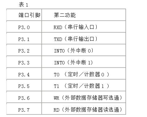
• Port 3: Port 3 is a set of 8-bit bidirectional I/O ports with internal pull-up resistors. The P3 output buffer stage can drive (absorb or output current) four TTL logic gates. When a “1†is written to port P3, the internal pull-up resistor pulls them up and acts as an input port. At this time, the P3 port pulled externally will use pull-up resistor output current (IIL).
In addition to being a general I/O port, the P3 port is more important for its second function, as shown in Figure 1:
In addition, port P3 also receives some control signals for FLASH flash memory programming and program verification. RST: Reset input. When the oscillator is operating, the microcontroller resets when the RST pin is high for more than two machine cycles.
• ALE/PROG: When accessing external program memory or data memory, the ALE (Address Latch Enable) output pulse is used to latch the address of the lower 8-bit byte. In general, ALE still outputs a fixed pulse signal at 1/6 of the clock oscillation frequency, so it can be used to achieve external clock output or for timing purposes. An ALE pulse will be skipped each time the external data memory is accessed.
When programming Flash memory, this pin is also used to input programming pulses (PROG). The D0 bit can be set to the 8EH location in the Special Function Register (SFR) area. ALE operation can be prohibited. After this bit is set, only one MOVX and MOVC instruction can activate ALE. In addition, this pin will be pulled up a little bit. When the microcontroller executes an external program, ALE should be set to forbidden.
• PSEN: The program memory allows the PSEN output to be the read strobe signal from the external program memory. When the AT89C52 is fetched from the external program memory, PSEN is active twice per machine cycle. That is, two pulses are output. At this point, the PSEN signal is skipped twice when accessing the external data memory.
· EA/VPP: External access allowed. To make the CPU only access external program memory (address 0000H-FFFFH), the EA must be kept low (grounded).
If EA is terminated at a high level, the CPU executes the instructions in the internal program memory.
When flash memory is programmed, this pin adds +12V to programming power supply VPP. The device must use 12V programming voltage VPP.
XTAL1: The inverting amplifier of the oscillator and the input of the internal clock generator. XTAL2: Output of the inverting amplifier of the oscillator.
The special function of AT89C52 is that in the AT89C52 on-chip memory, a total of 128 units of 80H-FFH are Special Function Registers (SFR). The address space map of SFR is shown in Table 2.
Not all addresses are defined, only 128 bytes from 80H-FFH are defined, and a considerable portion is not defined. Reading and writing to undefined cells will be invalid, the read values ​​will be indefinite, and the written data will be lost.
Data should not be written to undefined cells, since these cells may be assigned new functions in future products. In this case, these cell values ​​are always "0" after reset.
In addition to the AT89C51's all-timer/counter 0 and timer/counter 1, the AT89C52 also adds a timer/counter2. The Timer/Event Counter 2 control and status bits are located at T2CON, T2MOD. The register pair (RCAO2H, RCAP2L) is the Timer 2 capture/auto-reload register in either 16-bit capture mode or 16-bit auto-reload mode.
4, STC microcontroller minimum system
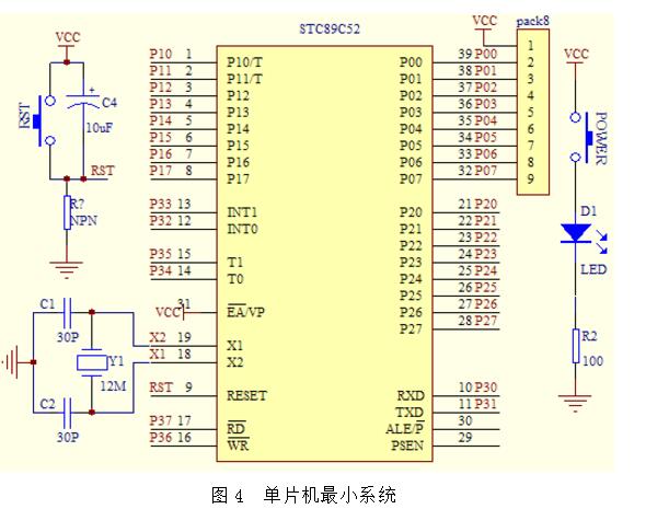
STC MCU is a high-performance, low-power 8-bit CMOS microprocessor chip, although STC microcontroller is powerful, but to complete its powerful features, it is not only depends on it, so let it run, It is necessary to create the environment for its work, that is, the minimum system. The minimum system of the STC microcontroller is shown in Fig. 1. It consists of an oscillation circuit consisting of a crystal and two capacitors, a reset button, a 10 UF capacitor and a 10 K resistor. The power circuit consists of three circuits. The system uses the STC89S52 single-chip microcomputer as its core and uses a crystal oscillator of 11.0592MHZ. The reset circuit is a key-high reset.
Second, system hardware circuit design1, crystal oscillator circuit
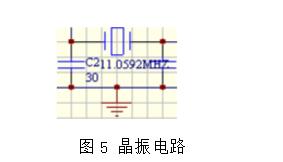
In the crystal oscillator circuit, C1 and C2 are the load capacitors of the crystal oscillator, which are connected to the two feet of the crystal oscillator and the capacitance to the ground respectively. The circuit is taken as 30PF. Because the XTAL0 pin and the XTAL1 pin in the oscillation circuit of the crystal oscillator and the microcontroller generate chopping waves, although the harmonics have little effect on the circuit, it will affect the stability of the clock oscillator in the circuit. Connecting two 5pf-30pf ceramic capacitor capacitors between the XTAL0 pin and the XTAL1 pin can increase the stability of the circuit.
2, reset circuit
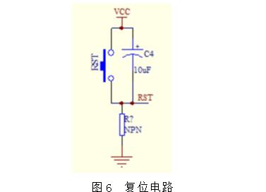
The microcontroller reset circuit has two methods: power-on reset and manual reset. Power-on reset requires a reset operation after the power is turned on. Manual reset requires the power supply to be turned on. Under the condition that the SCM is operating, during the operation of the SCM, the SCM is reset by using the button switch operation. This is a manual reset.
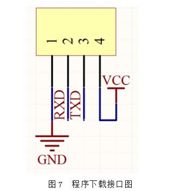
3, program download interface
1) 1602 LCD Overview
1602LCD means that the displayed characters and numbers are 16X2, that is, it can display two lines, each line of 16 characters LCD module a total of 32 characters and numbers.
1602LCD main technical parameters:
1. Display size: 16&Times; 2 characters
2. Chip rated voltage: 4.5-5.5V
3. Rated current: 2.0mA (5.0V)
4. Operating voltage: 5.0V
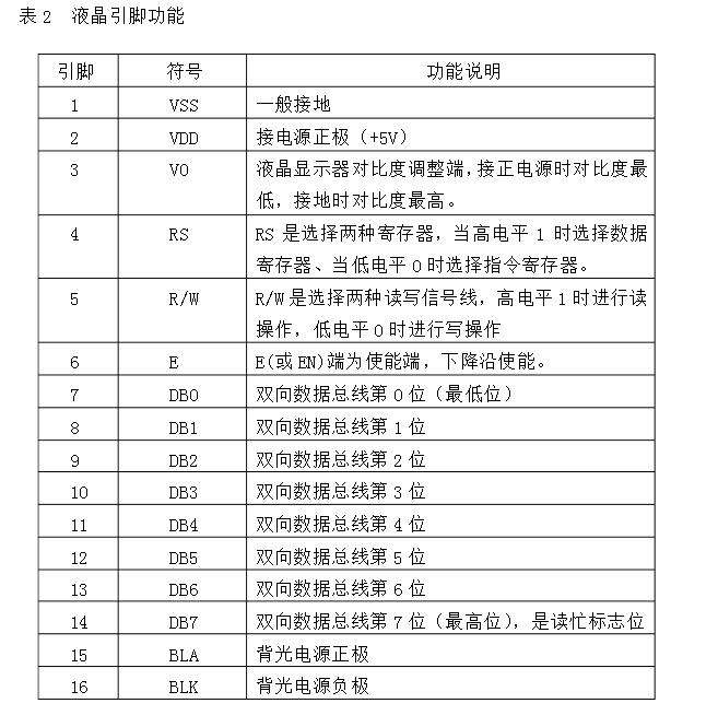
2) 1602 LCD pin function
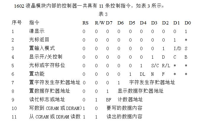
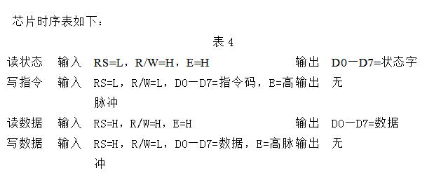
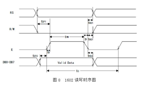
3) 1602 read and write timing diagram
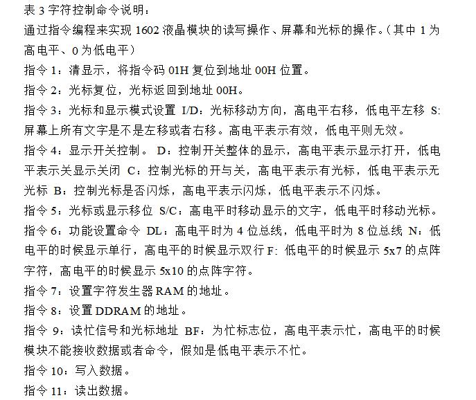
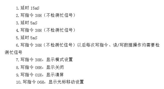
4. General initialization (reset) process of 1602 LCD
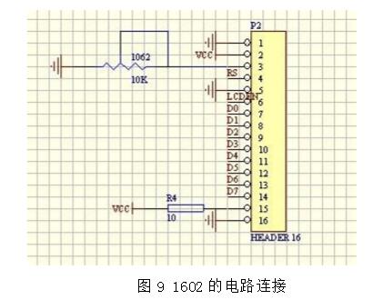
5, 1602LCD circuit connection
The liquid crystal terminal 5 is a read/write selection terminal. Since we do not read data from the liquid crystal and only write commands and display data to it, this terminal is always selected as a write state, ie, low level ground. The liquid crystal terminal 6 is an enable signal and is a signal necessary for operation. Its circuit is shown in Figure 2-11:
1) DS12C887 Overview
DS12C887 has a DS12R885 die, 32.768HZ quartz crystal and a rechargeable battery in three parts, DS12C887 is compatible with clock chips MC146818B and DS12887 commonly used by computers, and can be directly replaced. DS12887 can be used to directly replace the clock calendar chip on IBM PC. . The clock circuit designed with the DS12C887 chip has a good microcomputer interface and does not require any peripheral circuits and devices. The clock chip DS12C887 has the following features:
(1) The DS12C887 comes with a lithium battery. When the external power fails, the internal information can still be maintained for 10 years to ensure that no data is lost.
(2) Time information such as seconds, minutes, hours, days, weeks, days, months, years, and centuries can be generated automatically, and there is a leap year compensation function. It also added a century register internally and used hardware circuits to solve the "millennium" problem.
(3) It has two methods of expressing time, binary date and BCD code, calendar and timed alarm function.
(4) Time records in one day have two types of 12-hour and 24-hour clocks. In the 12-hour clock mode, PM and AM are used to distinguish between morning and afternoon. At the same time, the summer time mode can be selected.
(5) There are 128 RAM units and software interfaces, of which 11 bytes of RAM are used to store time information, 4 bytes of RAM are used to store the control information of the DS12C887, which are called the control registers 14 as byte clocks and control registers. 113 bytes of general-purpose RAM are used by the user.
(6) The user can also program the DS12C887 to achieve a variety of square wave outputs and block the internal three-way interrupts through software.
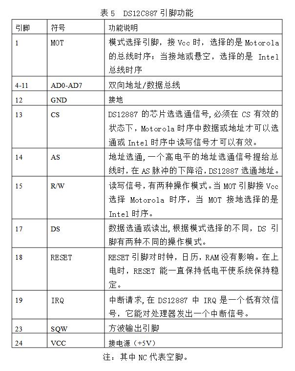
2) DS12C887 pin function
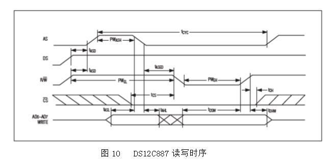
3) DS12C887 read and write timing
4) DS12C887 flow chart
After entering the main program, DS12C887 first initialize settings, when the serial port has data, then call the function to get calendar clock information from the calendar clock chip, call the display function to display the calendar clock information is displayed and repeated. This section includes the contents of a unit of DS12C887 that writes and reads DS12C887. 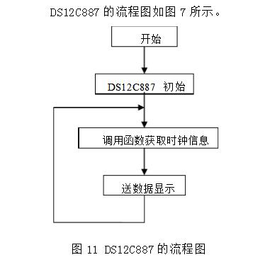 And DS12C887 set the time.
5) Clock chip pin introduction
1) Clock chip DS12C887, its pinout is shown below
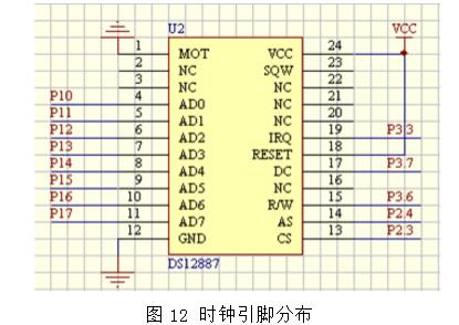
MOT (1 pin): Bus timing mode select pin. When connected to a high level, the MOTOROLA bus is selected to operate; when the pin is low or floating, the chip operates according to the INTEL bus. At this time, the timing of its operation is synchronized with the off-chip RAM read and write timing of the MCS51 chip.
NC (2,3,16,20,21,22 feet): No pin is understood. AD0~AD7 (4~11 pins): Address/address data multiplexed bus pins.
CS (13 feet): Chip select pin, active low.
AS (14-pin): Address latch input pin. Positive pulses on the pins are used to switch the address/data multiplexed bus. The trailing edge of the pulse locks the address into the DS12887. In the Intel bus mode, this pin is equivalent to the ALE pin of the MCS-51 series microcontroller chip.
R/W (15 feet): Read/write input pin. There are two operating modes for this pin. In the mode of selecting MOTOROLA bus, this pin is used to indicate the current read/write cycle, high level indicates a read cycle, and low level indicates a write cycle; when the INTEL neutral line timing mode is selected , This pin is an active low input pin, equivalent to the write enable signal (/WE) of general-purpose RAM.
DS (17-pin): This pin has two working modes. When the MOT is connected to the high level, this pin is the data latching pin. When the MOT is connected to the low level, this pin is the reading input pin. In the 51 system, Ds is equal to the RD pin. ·
RESET (18-pin): Reset input. When RESET is low and VCC≥4.25, the DS12C887 chip performs a reset operation. The voltage on this pin does not affect the contents of the clock, calendar, and on-chip RAM.
IRQ (19 feet): Interrupt request output pin, active low, as long as the status bit that caused the interrupt is valid and the corresponding interrupt enable bit is 1, the IRQ goes low. The microcomputer needs to read the register C to clear the pin signal, and the RESET pin can also clear the signal.
SQW (23 feet): square wave signal output pin. This signal output can be turned off by setting register bit SQWE. The output frequency of this signal can also be changed by programming the internal register of the chip.
VCC (24-pin): +5V power supply. When Vcc ≤ 3v, the chip will automatically switch Vcc to the built-in battery. When VCC recovers to 4.25V, it must be 100ms to access it.
6) Introduction to 4 control registers
The DS12C887 has four control registers that can be accessed at any time, even in an update cycle.
The contents of the register A byte are as follows.
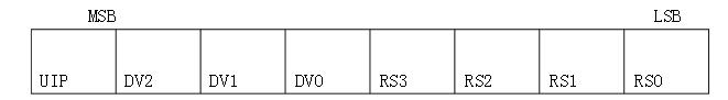
SET: set bit, can be read and written without being affected by the reset operation. When 0, it is not in the set state, the chip updates the time data; when it is 1, the data is suppressed from being updated, and the time and calendar information can be set through the program.
PIE: periodic interrupt enable bit, clear this bit on reset, can read and write. When 1, the cycle interrupt flag bit PF in register C is enabled, and the drive/IRQ pin outputs a low interrupt signal, and the cycle of the interrupt signal generation is determined by RS0~RE3.
AIE: Alarm interrupt enable bit, can read and write. When 1, the alarm interrupt flag AF in register C is enabled and an interrupt output is generated by the /IRQ pin when an alarm occurs.
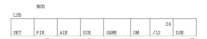
VRT; RAM and time effective bits. Used to indicate the status of the battery connected to the VBAT pin. This bit can not be written, nor affected by the operation, the general time to read always go to 1, if there is a read 0, it means that the battery is dead, the time data and RAM data will change Inaccurate.
The 113-byte ordinary RAM space of the chip DS12CR887 is a non-volatile RAM space that can be used as a non-volatile memory space in a non-processor program.
Alarm circuit
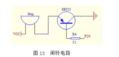
The alarm function is to output a square wave signal of a certain frequency from the I/O port of the single-chip microcomputer and drive the buzzer to send a sound signal with a specific frequency. When the time set by the alarm clock reaches the time of the clock, the microcontroller sends a low level to the buzzer, and the transistor turns on the driving buzzer to make a sound as a timed alarm.
Independent keyboard circuit
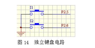
When the SCM detects that a button is pressed, it emits a binary coded signal corresponding to it.
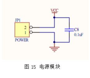
Power module
The clock is powered by a +5V DC power supply. In this design, four 1.5V batteries can be used. The schematic of the power supply module is shown in Figure 2-15.
High voltage
resistor dividers (RFD Series)
are suited for all the fields of high voltage and small signal multiply. Such as
Such as High voltage power
supply, Medical electronical devices,
Audiophile speakers, Audio systems, Smoke sensors, Infrared detectors, Radiation detectors, Special gas detectors
High Voltage Polyester Capacitor,High Voltage Divider,Flat High Voltage Divider,High Voltage Resistor Dividers,High Power Resistor
XIAN STATE IMPORT & EXPORT CORP. , https://www.shvcomponents.com