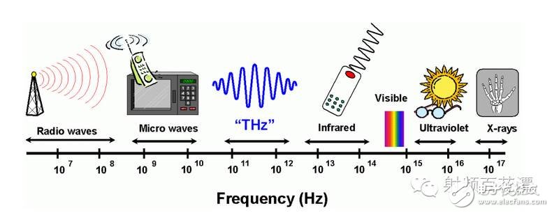
Millimeter wave technology and chip detailed
Due to the high cost of millimeter wave devices, they were mainly used in military applications. However, with the rapid development of high-speed broadband wireless communication, automobile assisted driving, security inspection, medical detection and other application fields, in recent years, millimeter waves have been widely studied and applied in the civilian field. At present, it is difficult to obtain a wide continuum spectrum for the gold communication band below 6 GHz, which seriously restricts the development of the communication industry. In contrast, the millimeter-wave band still has a large number of potentially underutilized spectrum resources. Therefore, millimeter wave has become a research hotspot of the 5th generation mobile communication. The 5th generation mobile communication research alternative frequency bands were identified at WRC2015 in 2015: 24.25-27.5 GHz, 37-40.5 GHz, 42.5-43.5 GHz, 45.5-47 GHz, 47.2-50.2 GHz, 50.4-52.6 GHz, 66- 76 GHz and 81-86 GHz, of which 31.8-33.4 GHz, 40.5-42.5 GHz and 47-47.2 GHz are permitted as co-option bands for specific use conditions. Various millimeter-wave devices, chips, and applications are in full swing. Millimeter waves have their own characteristics relative to the microwave frequency band. First, the millimeter wave has a shorter operating wavelength, which can effectively reduce the size of the device and system. Secondly, the millimeter wave has rich spectrum resources and can meet the needs of ultra-high-speed communication in the future. In addition, due to the short wavelength, millimeter waves have higher resolution for radar and imaging. So far, a lot of research has been carried out on millimeter waves, and various millimeter wave systems have been widely used. With the rapid development of civilian technologies such as the 5th generation mobile communication, auto driving, security inspection, etc., millimeter waves will be widely used in all aspects of people's daily lives.
In terms of millimeter wave technology, combined with some popular system applications of millimeter wave band, such as millimeter wave communication, millimeter wave imaging and millimeter wave radar, the development of millimeter wave chips is highlighted.
1, millimeter wave chipConventional millimeter-wave monolithic integrated circuits mainly use compound semiconductor processes, such as gallium arsenide (GaAs) and indium phosphide (InP), which have good performance in the millimeter wave band and are the mainstream integrated circuit process in this frequency band. On the other hand, silicon-based (CMOS, SiGe, etc.) millimeter-wave sub-millimeter-wave integrated circuits have also made great progress in the past decade. In addition, high-power high-frequency devices based on gallium nitride (GaN) processes are rapidly expanding to the millimeter-wave band. The following will be introduced separately.
1.1 GaAs and InP millimeter wave chips
GaAs and InP processes and devices have made great strides in the last decade. Millimeter wave device types based on this type of process mainly include high electron mobility transistor (HEMT), modified high electron mobility transistor (mHEMT), and heterojunction bipolar transistor (HBT). At present, the cutoff frequencies (ft) of GaAs, mHEMT, InP, HEMT and InP HBT exceed 500 GHz, and the maximum oscillation frequency (fmax) exceeds 1 THz. In 2015, Northrop Grumman reported that the InP HEMT amplifier operating at 0.85 THz, 2013 In the United States, Teledyne and the California Institute of Technology's Jet Propulsion Laboratory reported on InP HBT amplifiers operating at 0.67 THz. In 2012 and 2014, the Fraunhofer Institute for Solid State Physics in Germany reported mHEMT amplifiers operating at frequencies above 0.6 THz.
1.2 GaN millimeter wave chip
As a third-generation wide bandgap compound semiconductor, GaN has the advantages of large forbidden band width, high electron mobility and breakdown field strength. The device power density is more than 5 times that of GaAs, which can significantly increase the output power. Reduce size and cost. With the gradual maturity of GaN material preparation technology in the 1990s, GaN devices and circuits have become the hotspot in the development of compound semiconductor circuits. GaN is the focus of microwave and millimeter wave devices and circuits in the United States, Japan, and Europe. In the past decade, GaN's low-cost substrate material, silicon carbide (SiC), has also matured. Its lattice structure is matched with GaN and its thermal conductivity is good, which greatly accelerates the development of GaN devices and circuits. In recent years, GaN power devices have developed rapidly in the field of millimeter waves. Japan's Eudyna reported a 0.15 m gate length device with a power output density of 13.7 W/mm at 30 GHz. The US HRL reported several E-band, W-band and G-band. The GaN-based device has a W-band power density of more than 2 W/mm and a power density of 296 mW/mm at 180 GHz. Domestic GaN power devices in the microwave band have matured, and GaN power devices in the W-band have also made progress. The Ka-band GaN power MMIC developed by Nanjing Electronics Research Institute has a pulse output power of 15W in the 3436 GHz band, an additional efficiency of 30%, and a power gain of more than 20 dB.
1.3 Silicon-based millimeter wave chip
Silicon-based processes have traditionally been dominated by digital circuits. With the continuous development of deep sub-micron and nano-processes, the silicon-based process features continue to decrease in size, and the shortening of the gate length compensates for the lack of electron mobility, thereby increasing the transistor's cutoff frequency and maximum oscillation frequency, which makes the silicon process Applications in the millimeter wave or even the terahertz band are possible. The InternaTIonal Technology Roadmap for Semiconductors predicts that the feature size of the CMOS process will be reduced to 5 nm by 2030, and the cutoff frequency ft will exceed 700 GHz. The cutoff frequency ft and maximum of the SiGe process transistors from the German IHP Institute The oscillation frequency fmax has reached 300 GHz and 500 GHz, respectively, and the corresponding silicon-based process circuit can be extended to more than 200 GHz.
Due to the huge advantages of silicon process in terms of cost and integration, research on silicon-based millimeter-wave sub-millimeter-wave integrated circuits has become one of the current research hotspots. The University of Florida designed a 410 GHz CMOS oscillator. The University of Toronto, Canada developed a 170 GHz amplifier based on the SiGe HBT process, a 160 GHz mixer, and a 140 GHz CMOS-based inverter. The University of California, Santa Barbara, etc. The CMOS process developed a 150 GHz amplifier, and Cornell University developed a 480 GHz frequency multiplier based on a CMOS process. In terms of system integration, the University of Toronto designed the 140 GHz CMOS receiver chip and the 165 GHz SiGe on-chip transceiver system. The University of California, Berkeley, first integrated the 60 GHz band silicon-based analog transceiver circuit with digital baseband processing circuitry. On the CMOS chip, the Singapore Microelectronics Institute also implemented a 60 GHz CMOS transceiver chip including a chip antenna. The University of California, Los Angeles reported a frequency synthesizer of 0.54 THz. The Upattal University of Germany developed 820 GHz. The silicon-based SiGe active imaging system, the University of California at Berkeley, successfully developed the 380 GHz radar system using the SiGe process. Japan's NICT and other CMOS-based CMOS processes have implemented 300 GHz transceiver chips and achieved transmission rates in excess of 10 Gbps, but because of the lack of power amplification and low-noise circuitry, the transmission distance is very short. By using silicon-based technology, all circuits including digital circuits can be integrated on a single chip, which is expected to significantly reduce the cost of millimeter-wave communication systems.
In the millimeter-wave submillimeter-wave silicon-based integrated circuit, China has started late, but with the support of the National 973 Program, the 863 Program, and the Natural Science Foundation, research has been rapidly carried out and progress has been made. The National Key Laboratory of Millimeter Waves of Southeast University successfully designed Q, V and W band amplifiers, mixers, VCOs and W-band receivers, Q-band multi-channel transceivers, etc., and to 200 GHz based on 90 nm CMOS technology. CMOS multiplier and SiGe oscillator to 520 GHz.
2, millimeter wave electric vacuum deviceMillimeter wave integrated circuits have many advantages such as small size and low cost, but power is limited. In order to obtain higher output power, electric vacuum devices can be used. For example, Klystron developed by CPI of Canada has obtained pulse output power of more than 2000 W on the W band. The traveling wave tube developed by Beijing Institute of Vacuum Electronics (TWT) The pulse output power of the amplifier in the W band exceeds 100 W. The University of Electronic Science and Technology has also successfully designed the TWT power amplifier on the W band. The Gyrotron developed by the Hefei Institute of Material Science, Chinese Academy of Sciences was obtained at 140 GHz. The pulse output power of 0.9 MW is equivalent to the foreign level.
Mini Circuit breakers, also named as the air switch which have a short for arc extinguishing device. It is a switch role, and also is a automatic protection of low-voltage electrical distribution. Its role is equivalent to the combination of switch. Fuse. Thermal Relay and other electrical components. It mainly used for short circuit and overload protection. Generally, According to the poles, mini Circuit breaker can be divided into 1P , 1P+N , 2P, 3P and 4P.
Miniature Circuit Breaker,Electronics Miniature Circuits Breaker,Automatic Miniature Circuit Breaker,Mini Circuit Breaker,MCB
Wenzhou Korlen Electric Appliances Co., Ltd. , https://www.korlenelectric.com