Realization of electronic pricing scale application with high integration mixed signal single chip microcomputer
1. Introduction
Electronic weighing in life has gradually replaced traditional spring and day-to-day measurement tools, such as electronic pricing scales and electronic weight scales. The main components of the design electronic scale products are: sensor, ADC and MCU single chip. The electronic scale designed in this paper uses a pressure cell (Load Cell) to convert the pressure physical quantity into a voltage signal, and then converts the voltage into a digital display. Since the voltage is analog, it is converted to a digital signal by the ADC. At this time, the MCU single chip is also needed to control the signal processing and display functions on the electronic scale motherboard.
The HY16F188 control chip has built-in high-precision ΣΔ 24 Bit ADC, programmable Amplifier PGA and multi-stage regulated output, which greatly simplifies PCB peripheral circuits. The ΣΔ24 AD converter with high resolution, high resolution, and low temperature drift enables accurate analog to digital conversion. Although the output rate is not very high, it is not problematic for products such as electronic scales that do not require high conversion rates.
2. Principle description
2.1 Sensing component
The principle of Load Cell is to attach a strain gauge consisting of bridge resistors on the aluminum rod, namely the Wheatstone bridge, as shown in Figure 2-1. Because of the four resistors on the bridge (the same resistance), when a voltage is applied across VIN+ and VIN-, V+ = V-, that is, the bridge is balanced.
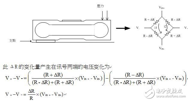
The resolution is divided into external resolution and internal resolution. The external resolution is the ratio of the output voltage value of the Load Cell full scale to the voltage value caused by the minimum weight to be identified. The minimum weight can be defined as 1g, 0.5g, 0.1g, etc. .
Internal resolution is an important indicator of the scale of electronic scales. Generally, the internal resolution determined by the visual method usually means that when the LCD display has only 1 grid scrolling, the full-scale grid number is the internal resolution, and the signal represented by 1 grid is about 2~ 3 times RMS Noise.
The smaller the ratio of internal and external resolution, the higher the accuracy of the electronic scale, but the ratio of internal and external resolution is limited. For example, the load cell full-scale pressure difference is 3mV, to achieve 3000 Count, the internal and external ratio of 1:10 electronic scale, if not amplified by the signal, the minimum signal to be processed is 3mV / (3000X10) = 0.1μV. The minimum signal value that ΣΔ24 can handle is about 65nV, so if the internal-to-foreign ratio is reduced, a signal will be generated that makes the ADC unrecognizable. If you use OPAMP, it will increase the cost. Therefore, the ratio of internal and external resolution should be stable within a certain range.
Whether the performance of the chip ADC can meet the specification requirements is usually based on RMS Noise to estimate whether the external stable internal resolution ratio. For the development of electronic scale products, the bottleneck of the maximum internal resolution that can be achieved with the HY16F188 chip is Input RMS Noise and not the resolution of the ADC. The ADC signal to be tested of HY16F188 is amplified by PGA, AD multiplier (PGA=32, ADGN=4), and the input RMS Noise is about 65nV under the condition that OSR=32768 outputs 10 ADC values ​​per second. However, since its Input Noise is mainly composed of Thermal Noise, if we pass the average software processing, Input Noise can be further reduced.
If we use an average of 8 software to process its Input RMS Noise is about 40nV, 3 times RMS Noise represents about 1 grid of scrolling, which is 120nV. When using 2.4V Load Cell drive voltage, 1mV/V Load Cell, the differential voltage can reach 2.4mV at full scale, so in this case we can get the internal resolution of 20000 Counts.
2.2 Control chip
Introduction to MCU: HY16F Series 32-bit High Performance Flash MCU (HY16F188)
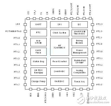
纮康HY16F series 32-bit high performance Flash microcontroller (HY16F188)
(01) Adopt the latest Andes 32-bit CPU core N801 processor.
(02) The voltage operation range is 2.4~3.6V, and the operating temperature range is -40°C~85°C.
(03) Support external 20MHz quartz oscillator or internal 20MHz high precision RC oscillator.
With a variety of CPU operating frequency switching options, users can achieve optimal power saving planning.
(3.1) Operating mode 350uA@2MHz/2
(3.2) Standby mode 10uA@32KHz/2
(3.3) Sleep mode 2.5uA
(04) Program memory 64KBytes Flash ROM.
(05) Data Memory 8KBytes SRAM.
(06) BOR and WDT function to prevent CPU crashes.
(07) 24-bit high accuracy ΣΔADC analog to digital converter
(7.1) Built-in PGA (Programmable Gain Amplifier) ​​up to 128 times magnification.
(7.2) Built-in temperature sensor.
(08) Ultra low input noise Rail to Rail op amp OPAMP.
(09) Multi-function CMP analog comparator and support 4 sets of hardware Touch Key function modules.
(10) 16-bit TImer A module.
(11) The 16-bit TImer B module has a PWM waveform generation function.
(12) The 16-bit TImer C module has the Capture/Compare function.
(13) Hardware SPI/I2C/UART serial communication module.
(14) Hardware RTC clock function module.
3. System design
3.1 Hardware Description
The analog signal output from the Load Cell is transmitted to the HY16F188. The MCU captures the AD signal value through its own ADC conversion. After the operation process, the corresponding weight value is obtained and displayed on the LCD. The 4X4 matrix key input can be used to perform related setting operations. , you can enter Sleep mode to reduce power consumption.
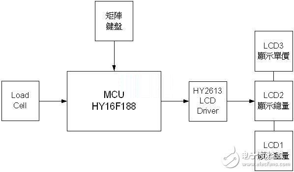
The overall application PCB motherboard is shown above.
(A) Central Processing Unit:
HY16F188 (Andes 32-bit MCU Core + HYCON 24-bit ΣΔADC + UMC 64K Flash)
The function is to measure the electrical signal, control, and operation including the function to store the calibration parameters.
(B) Display chip: HY2613 (HYCON LCD Driver LCD Segment 4X36)
Responsible for LCD driver.
(C) Power circuit: 9V to 3.3V power system.
(D) Analog sensing module: Load Cell.
(E) Online programming and ICE connection circuit, through the EDM connection, can support online burning simulation.
And has a strong C platform IDE and HYCON simulation software analysis tools and GUI support.
Patch panels are commonly used in computer networking, recording studios, and radio and television.
We are professional Network Patch Panel manufacturer in China. Our patch panel includes voice type 25port voice patch panel and 50port voice patch panel, data type (cat.5e,cat.6, cat.6a) with 6/12/24/48port on option. We use good PCD board and IDC connectors (krone IDC, 110 IDC, Dual IDC for option) to ensure the characters for each product. Specially for 24port Cat5e.UTP patch panel ,we offer not only in flat configuration as normal but also offer angel patch panels configuration.
The patch panel is offered universal wiring both T568A and T568B. We will do the Fluke test before selling our network patch panel.

Fiber Optic Patch Panel, Blank Patch Panel, Cat6a Patch Panel, Cat5e Patch Panel, Patch Panel Wall Mount
NINGBO YULIANG TELECOM MUNICATIONS EQUIPMENT CO.,LTD. , https://www.yltelecom.com