Stability standard for control systems
"Control Loop Design for Linear and Switching Power Supplies" is the latest work by Christophe Basso, a former columnist at Power Electronics. This work focuses on the knowledge that engineers really need to understand to compensate and stabilize a given control system. This article contains an excerpt from the book on stability standards.
In the electronics field, an oscillator is a circuit that produces a self-excited sinusoidal signal. In a wide variety of configurations, the acceleration process of the oscillator involves the noise inherent in the electronic circuitry that uses the oscillator. At the time of power-on, the noise level rises, and at this time, oscillation and self-excitation begin. Such a circuit can be composed of the constituent modules shown in FIG. As you can see, this configuration looks very close to the configuration of our control system.
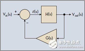
Figure 1: The oscillator is essentially an error signal that does not interfere with the control system of the output signal.
In our example, the excitation input is not noise, but the voltage level Vin, which is injected as an input variable to start the oscillator. The direct channel consists of the transfer function H(s) and the return channel contains the G(s) block. To analyze this system, we first write its transfer function by the equation of the relationship between the output voltage and the input variable:

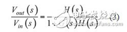
If we expand this formula and Vout(s), we get

Therefore, the transfer function of such a system is:
In this equation, the product G(s)H(s) is called the loop gain, which is labeled T(s). To convert our system to a self-excited oscillator, there must be an output signal even if the input signal has disappeared. In order to meet such a goal, the following conditions must be met:
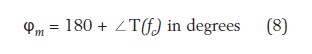
To verify this equation in the case of Vin disappearing, the quotient (quoTIent) must be infinite. The condition that the quotient is infinite is that the characteristic equation D(s) is equal to 0:
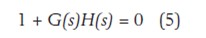
To satisfy this condition, G(s)H(s) must be equal to -1. In other words, the loop gain must be 1 and its sign should be changed to a negative sign. The sign change of a sinusoidal signal is simply a phase flip of 180°. These two conditions can be mathematically expressed in the following two equations:
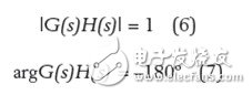
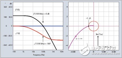
Figure 2: The oscillation conditions can be expressed in Bode plot or Nyquist plot.
Under the condition that these two equations are satisfied, we obtain the steady-state oscillation condition. This is the so-called Barkhausen standard, proposed by the German physicist Barkhause in 1921. In fact, in a control loop system, it means that the correction signal no longer resists the output, but returns in phase form with the same amplitude as the excitation signal. Equations (6) and (7) represent the loop gain curve in the Bode plot, which passes through the 0 dB axis and is affected by the 180° phase lag just at this point. In the Nyquist analysis, the relationship between the imaginary number of the loop gain and the relative frequency of the real part is plotted as a graph, which corresponds to -1, j0. Figure 2 shows two curves that satisfy the oscillation conditions. If the system deviates slightly from these values ​​(such as temperature drift, gain variation), the output oscillation will either drop exponentially to zero or the amplitude diverges until a higher or lower power rail is reached. In the oscillator, the designer tries to reduce the gain margin as much as possible so that the oscillation conditions can be satisfied under a variety of operating conditions.
Stable condition
As you know, the goal of the control system is not to build an oscillator. We want the control system to provide high speed, accurate and non-oscillating response. Therefore, we must avoid configurations that satisfy the oscillation or divergence conditions. One way is to limit the range of frequencies in which the system will react. By definition, the frequency range or bandwidth corresponds to a frequency that is 3 dB lower than the closed loop transmission channel from input to output. The bandwidth of a closed loop system can be viewed as a range of frequencies within which the system is considered to respond very well to its input (ie, to follow set points or to effectively suppress disturbances). As we will see later, in the design phase, we do not directly control the closed loop bandwidth, but control the crossover frequency fc - a parameter related to open loop analysis. These two variables are usually roughly considered equal, but we will see that this is only true under one condition. However, they are not too far apart, and the two can be interchanged in the discussion.
We have seen that the open loop gain is an important parameter in our system. When the gain is present (ie |T(s)|â€1), the system operates with a dynamic closed loop that compensates for input disturbances or reacts to setpoint changes. However, there are limits to the system response: the system must provide a gain at the frequency involved in the disturbance signal. If the disturbance of the setpoint change is too fast, the frequency component of the excitation signal is lower than the system bandwidth, indicating that these frequencies lack gain: the system slows down and does not react, and the operating state is like a loop that does not respond to waveform changes. So, is it asking for infinite bandwidth? No, because increasing bandwidth is like widening the diameter of the funnel: you can of course collect more information and react faster to input vibration, but the system will also receive spurious signals, such as converters. In some cases, the noise and parasitic parameters generated by itself (such as the output chopping in the switching power supply). Therefore, it is mandatory to limit the bandwidth to what your application really requires. Using too wide a bandwidth will impair the system's noise immunity (eg, it suppresses the robustness of external spurious signals).
Limit bandwidth
How do we limit the bandwidth of the control system? The method is to change the loop gain curve through the compensator block G. This block will ensure that the loop gain magnitude |T(fc)| falls below 1 or 0 dB after a certain amount of frequency fc. As we explained, once the loop is closed, it is roughly the bandwidth of your control system. The frequency at which this occurs is called the crossover frequency and is labeled fc. Is this enough to get a robust system? No, we need to make sure that another important parameter: the phase T(s) of the point with amplitude 1 must be lower than -180°. From our experiments, we have seen that when the loop gain is below -180° at the crossover frequency, we obtain a response towards steady state convergence. This is clearly a feature that our control system wants. To ensure that we avoid -180° during crossover, the compensator G(s) must customize the loop argument at the selected crossover frequency to construct the phase margin (PM or φm). . The phase margin can be viewed as a design or safety constraint to ensure that loop gain changes do not destabilize even in the presence of external disturbances or unavoidable producTIon spreads. As we will see later, the phase margin also affects the transient response of the system. Therefore, the choice of phase margin does not depend solely on stability considerations, but also on the type of transient response you expect. The mathematical definition of the phase margin is as follows:
Where T represents the open loop gain, including the graded body H and the compensator G gain.
A typical loop gain curve for classical compensation is shown in Figure 3, which shows a crossover frequency of 6.5 kHz. At this point, the T(s) phase is -90°. If you want to start at -180° at 6.5 kHz and positively count the phase degrees until you cross the amplitude waveform, you get a 90° phase margin in this example. This is an extremely robust system that is considered to be stable under all conditions: even if the loop gain is somewhat changed near the crossover point, it is impossible to cross the frequency where the phase margin is too small. The so-called "too small", we mean that the phase margin is close to the 30 ° limit, below which the system provides an unacceptable ringing response. That's why you learned that 45° is the limit when you go to school, and this value provides extra margin compared to 30°. We will see the source analysis of these numbers later.
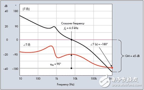
Figure 3. In this example, the 0 dB crossover point is at 6.5 kHz, and the total phase lag at this frequency provides a phase margin of 90°
Gain margin and stability conditions
Figure 4 shows another typical frequency response of the compensated converter, highlighting the 0 dB crossover point and phase margin. As we know from experience, the components that make up the converter reproduce performance changes over the life of the generator. These changes may be caused by normal production differences (eg resistance or capacitance is subject to different batch-to-batch tolerances). The environmental operating conditions of the converter also have an effect on the components. Among these variables, temperature plays a key role in affecting passive or active component parameters such as capacitance or inductive equivalent series resistance (ESR), optocoupler current transfer ratio (CTR), or beta of bipolar transistors. These variables affect the loop gain, causing it to rise or fall, depending on the parameters being affected.
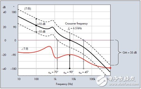
Figure 4. The loop gain shows sensitivity to external parameters such as temperature. When there is a change, the phase margin must always remain within the safety limits.
If the gain curve changes, the 0 dB crossover frequency will transition to the new value, applying a different bandwidth to the converter. How will the stability of the converter be affected under these changing conditions? If the new crossover frequency occurs at a point where the phase margin is small, the transient response performance may drop, making the overshoot no longer acceptable. Therefore, as a designer, your responsibility is to ensure that these dispersions do not suddenly increase the gain as you approach the -180° limit. You need ample gain margin, which is defined as follows:

It corresponds to a frequency point of exactly -180° or radians (1 MHz in Figure 3).
Figure 4 depicts a typical gain variation of ±10 dB due to the range of production variations of selected components. It brings a crossover frequency from 1.5 kHz to 30 kHz. In this region, the phase margin is changed from 70° to 45°, which are theoretical safety figures. What is the worst case? That is, the new crossover frequency occurs at a total phase lag of 180°. This condition comes out at 1 MHz, indicating a positive gain change of 35 dB.
Less likely to have large gain
Advantageously, a gain variation of 35 dB is less likely to occur in today's electronic circuits. Previously, when a transformer or servo system was driven by a vacuum tube circuit, the warm-up time during the power-up sequence may cause large loop gain variations. Therefore, the gain specification necessitates the rejection of a second point where there may be a risk of stability. This gain margin is seen on the loop gain curve at a frequency where the total phase lags by -180°, which is labeled GM in Figure 3. In today's electronic circuits, a gain margin of more than 10 dB is usually sufficient unless your loop gain is extremely sensitive to external parameters.
Another example of gain drift is shown in Figure 5. The figure shows another compensated converter with an 80° phase margin at 10 kHz. Based on the discussion above, we know that gain variations may occur, causing the gain curve to go up or down. In our example, we can see that the phase margin of an area around 2 kHz is as small as 18°. If a 20 to 25 dB gain drop occurs, the resulting control system will have a rather dangerous low phase margin of about 2 kHz. This will result in an oscillating response that is likely to exceed the overshoot specification. Such systems are considered conditionally stable. Advantageously, as mentioned earlier, a gain variation of 25 dB is not common, and systems with such gain margins can be considered robust. However, I have seen in some design cases that the end user (your customer) clearly indicates in the specification that it does not accept conditional designs, requiring phase margins greater than 60° at all points below the crossover frequency. In this case, the compensation converter is forcibly required so that there is no region where the phase margin is lowered, regardless of the operating conditions, below the crossover frequency.
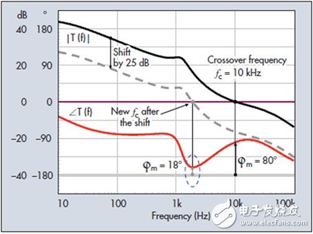
Figure 5. In this example, if the gain drifts below 25 dB, the curve crosses the 0 dB axis at a frequency point where the phase margin is only 18°. Such a phase margin will be affected by large disturbances, providing an extremely oscillating response. This is the case of conditional stability.
Stable, or unstable?
It is generally believed that a system that drops to below -180° before the crossover is an unstable system. Such a response is shown in Figure 6. The phase curve drops rapidly after 1 kHz and crosses the limit of -180° in the range of several kHz after 1.5 kHz. The phase curve then rises again, providing a 50° phase margin at 10 kHz. Yes, this system is very stable, simply because we do not satisfy equation (7) at 0 dB. It is important to remember that to eliminate the denominator of equation (3), you must make the gain size exactly equal to 1 and the phase lags 180° or more. In the figure, we can see that any point does not satisfy this condition. However, it is worth mentioning that this loop is highly conditional. If the gain is reduced by a few dB, your phase margin will become lower than 45°. The gain is further reduced by 10 dB and you will enter a hazardous area with a phase margin of 0, at which point the oscillation condition will be reached.
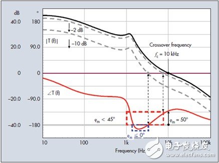
Figure 6. The phase lags by 180°, but in the region where the gain is greater. This does not constitute a problem and its response is acceptable.
Note: This article was approved by the publisher Artech House, Inc., Boston and is excerpted from the book Linear and Switching Power Supply Control Loop Design Tutorial (c) 2012. The topics of this book include: loop control basics, transfer functions, control system stability conditions, compensation, op amp-based compensation, transconductance-based compensation based on operation, TL431-based compensation, and flow stabilization Pressure-based compensation, measurement and design examples. This book can be purchased on ArtechHouse.com, Amazon.com or BN.com.
2020 Hottest Cob Grow Light diy model, 200w grow light , cob grow light, high power grow light, etc.
Can also do OEM/ODM service, More cob Led Grow Lamp is a great ideal for all kinds of indoor garden plants: lettuce, orchid, organic herbs, pepper, strawberries, succulent, hydroponic, medical plants.
Whether it's hydroponics, plants in soil, you can add a touch of magic to every veg and flower with Xeccon grow lights.


Cob Grow Light,Best Cob Led Grow Light ,Grow Light Cob Diy,Diy Grow Light
Shenzhen Wenyi Lighting Technology Co., Ltd , https://www.wycngrow.com