Application of LED Packaging Technology in Practice Teaching of Photoelectric Engineering
1 Introduction
With the continuous deepening of people's understanding of engineering education issues, experimental and practical teaching in engineering higher education has received more and more attention. However, how to reflect professionalism, research and innovation in the specific implementation of experimental and practical education is indeed an important issue that everyone faces. As we all know, the level of education investment in China has been relatively low, and the photoelectric-related experimental equipment is generally very expensive, especially for nanotechnology, high-speed optical communication and so on. Due to the particularity of practical teaching itself, it is generally required to complete a large number of students' practice training in a short period of time. The number of sets of instruments needs to be sufficient; within a limited budget, the price of each instrument must be very low. This has made us more limited in the setting of practical content. After many investigations, we selected LED (Light Emitting Diode) package as one of the practical teaching content. After more than a year of practice, it proved to be effective. LED is a kind of light-emitting device that can directly convert electric energy into visible light and radiant energy. It has low working voltage, low power consumption, high luminous efficiency, short response time, pure light color, firm structure, impact resistance, vibration resistance and performance. It has a series of advantages such as stable and reliable, light weight and small volume. It has developed rapidly and can now mass produce high-brightness and high-performance products of various colors in the visible spectrum. The application prospect is broad.
2 LED package internship meaning
The advancement of society and the development of science and technology have become more and more demanding for energy. Limited energy resources have intensified the energy crisis. Energy shortage is a prominent bottleneck restricting economic development in today's society and for a long period of time in the future. The Fifth Plenary Session of the Central Committee proposed to save resources as a basic national policy. The 11th Five-Year Plan outlines a 20% reduction in energy consumption per unit of GDP during the 11th Five-Year Plan period as a binding indicator. In June 2007, the State Council specially formulated the "Comprehensive Work Plan for Energy Conservation and Emission Reduction". The National Development and Reform Commission and the National High-tech Industry Bureau actively promoted and promoted the development and promotion of new energy and energy-efficient products. The long life of LEDs of 100,000 hours will greatly reduce the maintenance cost of LED lighting, reduce power consumption and carbon dioxide emissions.
In recent years, Japan's Nichia, Toyota Synthetic, SONY, Jiayou Electric, etc. have already appeared LED lighting products. World-renowned lighting companies such as Philips, Osram, GE, etc. have also invested a lot of manpower and resources in the research and development and production of LED lighting products. GE and EMCORE have partnered to form a new company to develop white LEDs to replace incandescent, compact fluorescent, tungsten halogen and automotive lamps. China is currently one of the fastest-growing countries in the world, with many companies engaged in research and production of LEDs. It is expected that in the next few decades, the market demand for high-power, high-brightness, energy-saving LED lighting products is extremely large.
Graduation internship is a compulsory practical teaching link for every engineering student. In order to achieve the training goal of undergraduate education, design a set of LED package internship system based on the principle of easy to use, reduce cost, and perfect the connotation of LED packaging process. Through the existing equipment to complete the practice of nearly 30 processes from crystal expansion, dispensing, solid crystal, baking, wire bonding, potting, etc., so that students can fully understand the packaging principle and specific process of integrated circuits and semiconductor optoelectronic devices process. In the past experiments, students can often access the contents of the device and components to the instrument level. Through the practice of the complete packaging process, students can use their own hands to operate semiconductor chips of only a few hundred microns. I can really feel the problems that I can't understand by reading or reading an article. It lays a good foundation for the research of photonic crystals and nanodevices in the graduate stage. Inspired by the problems of fixing and connecting tiny devices in future work or research, I opened a window for the students to touch the world of chips. At the same time, feel the process in the scale production process, so that they form a preliminary engineering concept.
3 LED packaging process
In the LED industry link, upstream is LED substrate wafer and substrate production, midstream is LED chip design and manufacturing production, downstream is LED packaging and testing. The development of low thermal resistance, excellent optical characteristics, and high reliability packaging technology is the only way for new LEDs to become practical and market-oriented. In a sense, it is the link between the industry and the market. Only the package can become a terminal. Products, put into practical use.
LED packaging technology is mostly developed and evolved on the basis of discrete device packaging technology, but it has great speciality. In general, the die of the discrete device is sealed within the package, and the package functions primarily to protect the die and complete the electrical interconnection. The LED package not only needs to complete the output light, but also protects the normal operation of the die. It has both electrical parameters and optical parameter design and technical requirements. It is not possible to simply use the package of the discrete device for the LED.
The production and manufacture of LED products has a complete and rigorous process, and each step has a direct impact on the final performance of the product. The basic flow chart of the LED package is shown in Figure 1.
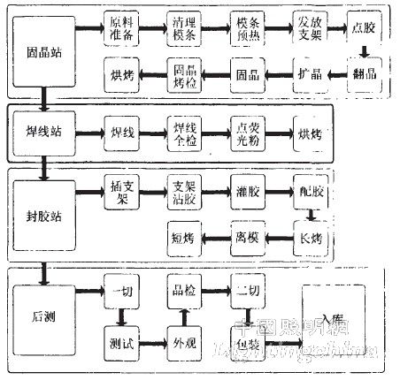
Figure 1 LED package flow chart