Design of DSP Control System Based on EMIF Interface
Abstract: This paper proposes a scheme for DSP to control complex systems through EMIF interface. By connecting the DSP chip to multiple FPGAs and using FPGAs to connect with various external chips, the DSP can control various chips through the EMIF interface to realize control of complex systems. This saves the DSP's pin resources and allows the DSP's computing functions to be fully utilized.
1 Introduction
With the development of information technology, digital signal processing technology has become one of the most important technologies in the digital society. Due to its high speed, high stability and low power consumption, digital signal processors (DSPs) have been widely used in communication, image processing, and automatic control in recent years. Among them, Texas Instruments' TMS320 series DSPs occupy a major share of the world DSP market, and TI has become the world's largest DSP manufacturer. This system uses the TMS320C6722 floating point DSP chip.
The EMIF Interface (External Memory Interface) is a high-speed interface on the TMS320 series of DSPs. It was originally designed to achieve high-speed connections between DSPs and different types of external expansion memories (such as SDRAM, FLASH, etc.). In some current applications, in order to fully utilize the computing power of the DSP and expand its pin resources, engineers often use the EMIF interface to connect to the FPGA, and then connect to various external devices through the FPGA. In this way, the FPGA becomes a transfer station, and the data of various digital chips can be transmitted to the DSP through the FPGA. For more complicated systems, when the pin resources of an FPGA chip are exhausted, it can be on the EMIF interface of the DSP. Connect multiple FPGA chips and connect differently-functioning chips to the FPGA. This way, the DSP chip can control complex systems only through the EMIF interface.
2 DSP+FPGA system implementation based on EMIF interface
2.1 System Architecture
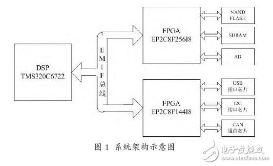
Figure 1 is the system I used. The DSP chip is connected to two FPGAs through the EMIF interface. The EP2C8F256I8 is mainly responsible for the exchange of data required by the DSP core processing, and is connected to the FLASH chip, the SDRAM chip, and the A/D chip. Another FPGA chip EP2C8F144I8 is responsible for external communication, connecting USB interface chip, I2C communication chip and CAN bus communication chip.
The EMIF interface of the TMS320C6722 DSP is designed to be connected to an external expansion memory. The EMIF interface has two modes of operation: SDRAM mode and asynchronous mode. The SDRAM working mode is a synchronous working mode designed for SDRAM. The EMIF interface can automatically refresh the SDRAM. The asynchronous working mode is a mode used when working with asynchronous devices such as SRAM and FLASH. In this department

Figure 2 shows the interface between the DSP and an FPGA. When the DSP is connected to multiple FPGAs, the interface can be multiplexed as shown. The EMIF interface of the TMS320C6722 DSP has 14 address lines. When communicating with different FPGAs, To use a different address.
2.2 DSP and FPGA communication timing
2.2.1 Asynchronous read operations
When the DSP issues a read request to the FPGA, an asynchronous read operation is performed. When a read operation cannot be completed within one access cycle of an external device, the EMIF performs multiple cycles of operation until the entire application is completed.
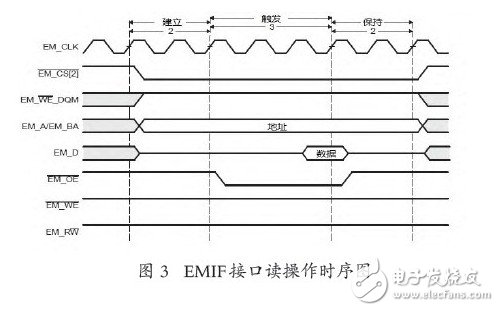
An EMIF read operation is divided into three parts: setup time, trigger time and hold time. At the beginning of the setup time, the EM_CS[2] chip select signal is pulled low, while the address lines EM_A and EM_BA give the address of the read data. At the beginning of the trigger time, the EM_OE signal is pulled low and the FPGA transmits data on the EM_D signal line. The DSP will sample the data at the last clock of the trigger time. The EM_OE signal will be pulled high during the hold time and the EM_CS[2] signal will be pulled high after the hold time has elapsed. The EM_WE_DQM, EM_WE, and EM_RW signals are always high during the entire cycle.
2.2.2 Asynchronous Write Operations
When the DSP issues a write request to the FPGA, an asynchronous write operation is performed. When a write operation cannot be completed within one access cycle of an external device, the EMIF performs multiple cycles of operation until the entire application is completed.
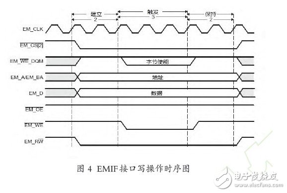
Similar to read operations, EMIF write operations are divided into three parts: setup time, trigger time, and hold time. At the beginning of the setup time, the EM_CS[2] chip select signal is pulled low, the EM_RW signal is pulled low, and the address lines EM_A and EM_BA give the address of the read data, and the data line EM_D gives the data that needs to be written to the FPGA. At the beginning of the trigger time, the EM_WE signal is pulled low and the EM_WE_DMQ signal gives the byte enable signal. The EM_WE_DMQ signal and the EM_WE signal are pulled high at the beginning of the hold time, and after the hold time is over, the EM_CS[2] signal and the EM_RW signal are pulled high. The EM_OE signal is always high during the entire write cycle.
The DSP implements the above timing by configuring the registers of the EMIF interface. The FPGA can implement the EMIF protocol by using an IP core. Different FPGA chips must use different addresses.
3 system BOOT method
There is no writable ROM inside the TMS320C6722 DSP. The DSP program must be stored in an external device. After the DSP chip is powered on, the program must first be downloaded from the external chip. This DSP can be started via the SPI bus, booted via the I2C bus, and booted via the EMIF interface. These kinds of Boot methods and corresponding pin configurations are shown in Table 1. In this system, in addition to the usual data exchange, the EMIF interface also functions as a DSP-enabled device.

After the system is powered up, the RESET pin of the DSP should be pulled low by the pull-down resistor to put the DSP in the reset state. After the FPGA chip EP2C8F256I8 is powered on, the program is started by downloading from the FPGA configuration chip EPCS4. After the FPGA is successfully booted, pull the SPI0SOMI pin of the DSP chip and the SPI0CLK pin low, pull the SPI0SIMO pin high, and then pull the RESET pin high. This configuration is to enable the DSP to start up through the EMIF interface based on the above three pins when the DSP exits the reset state. After that, the DSP chip will read 1KB of data from the EMIF interface, and store the 1KB of data in the RAM of the DSP, and then execute the 1KB program.
The above process is called the first startup process of the DSP. This 1KB program is written in assembly language and compiled into machine language by CCStudio software and stored in FPGA (program compiled into FPGA via mif file). The function of the 1KB program is to call the EMIF interface again, operate the FPGA, and make the FPGA copy the rest of the program (the program of this system is about 32K) from the FLASH chip into the RAM of the DSP through the IP core and execute these newly copied programs. . This is the second launch of the DSP. The first boot is hardware boot, which is the boot mode set by the TMS320C6722 DSP. The second boot is software startup, and the startup program executed is written by the user.
In summary, this paper introduces the hardware circuit and timing of the DSP chip connected to the FPGA through the EMIF interface. According to the method described in this paper, the DSP chip can control a large number of external chip operations through the FPGA, and only the DSP EMIF interface can realize the DSP startup and control complexity. The function of the system greatly expands the flexibility of the DSP chip, so that its powerful computing functions can be better played.
Heavy weight belting products are available in multiple widths and styles. Most of the heavy weight fabrics are heavily coated with PTFE to ensure consistent and reliable release performance. Besides that, its outstanding performance in wear resistance, coefficient of friction and compression strength make it suitable for diverse applications as polymer casting, lamination, composite manufacturing, rubber curing.

PTFE Conveyor Belts,Fiberglass Conveyor Belt,Non Stick Conveyor Belts,PTFE Coated Conveyor Belt
TAIZHOU YAXING PLASTIC INDUSTRY CO., LTD , https://www.yaxingptfe.com