High performance multi-level LED driver design for efficient linear dimming
The basic LED driver for general lighting applications is relatively simple, but when additional functions such as phase cut dimming and power factor correction are required, the design becomes very complicated. Non-dimming LED drivers without power factor correction typically include an off-line switching power supply that is tuned for constant current output. This is not much different from standard off-line switching power supplies and models that are common in AC-DC adapters. This design can use standard SMPS (switching power supply) circuit topologies such as buck, boost or flyback converters.
On December 3, 2009, the US Department of Energy (DOE) released the final version of the "Energy Star" specification for the integrated LED lamp project, stipulating that the power factor of LED drivers used in the United States must be better than 0.7, while industrial applications It is expected to be better than 0.9. Many products in the current market can not meet such requirements, so the future needs to be replaced with more advanced products. There are two ways to implement power factor correction (PFC), each requiring additional circuitry at the front end of the power converter: a simple low-cost passive PFC, and a more complex active PFC.
Before delving deeper into these methods, one thing to emphasize is that in order to receive an ENERGY STAR rating, the LED driver must be dimmable.
In general, this means that the adjustability will be derived from the existing wall-type electronic dimmer based on the principle of phase-cutting. This principle was originally designed to design pure-impedance incandescent lamps. While other dimming methods, such as linear 0-10V dimming or DALI, may be desirable, they may all be limited to high-end industrial LED drivers. So far, the application of phase-cut dimmers is quite extensive, and it is clear that LED lamps that can effectively dim will have great advantages. Since there are many low-cost dimmers based on triacs on the market, it is unrealistic to ensure that LED drivers are compatible with all categories. In particular, many dimmers use only basic designs and have very limited performance. For this reason, the ENERGY STAR program only requires LED driver manufacturers to specify in a web page which dimmers are compatible with their products.
Another requirement worth noting in the ENERGY STAR specification is that the LED's operating frequency must be greater than 150 Hz to eliminate the possibility of visible flicker. This means that the output current to the LED cannot be supplied with any large amount of ripple that is twice the linear frequency (50 Hz or 60 Hz).
In off-line applications such as office lighting, public buildings and neighborhood lighting, Led Lighting is used in more and more applications and will continue to be in the next few years. In these applications, high-power LEDs will replace linear or high-power CFL fluorescent lamps, HID lamps, and incandescent lamps. These applications require an LED driver with a typical power range of 25W to 150W. In many cases, the LED load consists of a high-brightness white LED array, usually in a variety of chip packages. The DC current used to drive these loads is typically at least 1 amp. Actually there are also AC current driven LED systems, but DC systems are generally considered to provide better driving conditions for LEDs.
Galvanic isolation is required in led lighting equipment to prevent the risk of electric shock where it can be accessed, which can occur in most cases unless an insulated mechanical system is used. This is because, unlike fluorescent lamp lighting devices that do not require insulation to achieve safety, the LED chip needs to be connected to a metal heat sink. In order to achieve good thermal conductivity, it is necessary to form a thermal barrier between the LED chip and the heat sink, so that it is not necessary to add an insulating material to meet the insulation requirement. Therefore, it is the best choice to form insulation inside the LED driver, and it also shows that the power converter topology is feasible.
The two possible solutions are a flyback converter or a multi-stage converter including a PFC stage, followed by an isolation and buck stage, and finally a back-end current regulation stage. Among the two schemes, the flyback is widely used because of its relatively simple and low cost.
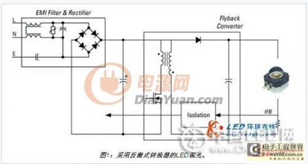
Flyback converters provide a good solution for many applications (Figure 1), however, they have the following limitations: limited power factor correction capability; limited efficiency over a wide input voltage range; twice the line frequency ( The output ripple at "150 Hz) is difficult to eliminate; dimming is required by an additional circuit.
Although the extra cost of multi-level design (Figure 2) limits its use in high-end products, this design can overcome some of these problems. It achieves high power factor and low total harmonic distortion (THD) over a wide range of AC output voltages, allowing the same LED driver to be powered from a mains supply of 110V, 120V, 220V, 240V or 277V.
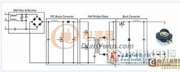
Figure 2: LED dimming with multi-level converter
It is able to maintain high efficiency over a wide range, rather than allowing the efficiency to peak at a particular line load point, but it drops dramatically under different conditions. At the same time, it is also easier to reduce the ripple output at 150Hz, and the multi-stage system makes it possible to use different dimming methods more efficiently.
The rest of this article will delve into the wide-voltage input range, insulation, dimming, and regulated DC output multi-level LED driver design principles, primarily for applications ranging from 25W to 150W. The multi-level LED driver in this example will be divided into three sections: front end, power factor correction (PFC) section; insulation and step down sections; back end, current modulation section.
The front-end section includes a boost converter that is pre-conditioned with a power factor correction that provides a high-voltage DC bus at the output that stabilizes it to a fixed voltage over a wide range of voltage or load variations. Due to the slow response of the regulated control loop, many cycles of the AC line frequency are subject to load variations, which only absorb a basic sinusoidal input current. This circuit typically works in critical conduction mode, otherwise it is considered a conversion mode. In this mode, the PWM turn-off period and the resulting switching frequency are variable, so that when all of the energy stored in the boost inductor is transferred to the output, a new switching cycle begins. This resonant mode of operation is widely used and achieves high efficiency due to its minimal switching losses. It is best to use this design within the specified power range.
The intermediate stage converts the high voltage DC bus voltage (typically around 475V) into a low voltage output suitable for driving the LED load. For safety reasons, LED loads are typically driven at low voltages, so the drive circuit typically has a minimum of 1 amp. The recommended insulation and buck stage configuration is a resonant half bridge that includes a pair of mutually inverting signals to drive the switching MOSFET. One end of the primary winding of the high frequency step-down transformer is connected to the two switches. The other end is connected to the capacitor crossover network of the DC bus to the ground loop. In this way, the transformer primary can see a square wave with equal positive and negative voltage amplitudes. The secondary winding will use a center tap so that two diode rectifiers can be used to convert the output current to DC. The output current is high enough to replace the rectifier diode with a MOSFET to operate as a synchronous rectification system. In a typical application with 3 amps of current, the surface temperature of the synchronous MOSFET is lower than the temperature of the Schottky diode in the same package at an ambient temperature of 30 degrees.
We can see that as the current requirements increase, the thermal advantage of synchronous rectification becomes more significant. Finally, a smoothing capacitor is needed to create an isolated low ripple DC voltage. The capacitance of this capacitor is on the order of tens of Farads, so ceramic capacitors are used.
In order to make the half-bridge stage more efficient, it should be designed to operate in resonant mode where the MOSFET is switched at zero voltage (ZVS) conditions. To achieve this, one must ensure that one MOSFET is turned off and the other MOSFET is turned on with a short delay, and that the delay voltage is commutated from one rail to the middle of the other. This is because the energy in the inductor is released and conducted through the body diode in the MOSFET. In the primary design of the transformer, it is necessary to maintain sufficient leakage inductance so that more energy can be stored and energy exchange can be performed. In this way, the design of the transformer becomes more complicated, and an easy way to avoid these problems is to use a standard high-frequency transformer design without adding extra leakage inductance to the design. It is only necessary to add another parallel to the primary inductance. An inductor to promote energy exchange. This additional inductor can also be used to help dimmers based on triacs and provide additional cost and space for adjustments. We will further explore this. Such inductors can use an open air gap core or an open core to increase energy storage.
The rear stage of the LED driver includes a current modulating circuit with short circuit protection. This can be done with a linear modulation circuit, but this is not enough. It is only suitable for low output currents and not for multi-level systems. The alternative is a simple buck regulator circuit that uses current feedback to limit each output current that exceeds the target LED drive current. This compensates for changes in the total LED forward voltage due to temperature and device tolerances, as well as currents in short-circuit or other fault conditions, protecting the drive from damage.
When multiple output stages are connected to a separate isolated DC voltage that is powered by the previous stage, a multi-stage channel can also be used. Because in such a design, an output short circuit in one channel does not hinder the normal operation of other channels. Moreover, this also allows the modulation currents of several channels to be provided to different LED arrays, and the need to connect parallel LED arrays is eliminated. It is well known that if LEDs do not have similar forward voltage drops at similar temperature conditions, then parallel connection of LEDs will present problems, and the advantages of using drivers with multiple independent outputs are obvious.
Disadvantages of TRIAC dimmers
Most existing dimmers typically operate in a leading edge phase-cut manner, using a very simple circuit based on a triac. These dimmers were originally designed to be used with incandescent lamps as resistive loads. A triac is a semiconductor switch that conducts current in either direction between its two main terminals only after it has been pulsed by its third gate. This pulse can have any polarity and is therefore easy to create with a basic RC timing circuit. The working principle includes triggering the triac at one point of the AC line cycle, so that it will be turned on until the end of the cycle, the linear voltage drop is zero at the end of the cycle, and then flows through the triac The switch current will also be zero and the triac will be turned off again. The triac has a minimum rated holding current below which the switch will turn off. The potentiometer in the regulation circuit controls the turn-on point of the triac in the regulator circuit and changes the overall average AC current by dimming.
However, even if they include a power factor correction front end, LED converters and other power supplies or electronic ballasts do not become purely resistive loads of the dimmer. When the dimming level is lowered, the triac in the dimmer may be excited or missed during the switching cycle. The factors that affect this performance are very complex, and since we have found a simple solution that can best overcome this problem in a multi-level system, there is no need for in-depth analysis here.
There is no need to return the rectified commutating inductor in the primary side of the step-down transformer to the midpoint of the capacitive divider, and the current can flow back to the line input through a DC split capacitor. This provides a small amount of additional current before the end of the AC line cycle, which will turn the triac on and allow it to operate within the required dimming range. This solution helps dimming by using a dimmer based on a triac based on the current that will be wasted. (image 3)
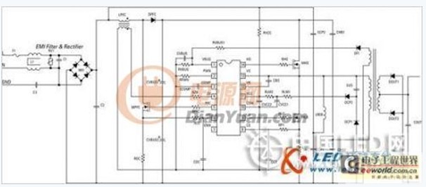
Figure 3: Front end and half bridge with dimming charge pump
Dimming in this way is practical, and as the dimming level is reduced, the output bus voltage of the front-end stage is also reduced. This causes the secondary voltage to also drop. Because the LED load has a fixed total voltage drop, a small change in voltage will also cause a large change in current and light output. In this way, linear dimming of the LED is achieved, meeting the requirements of more complex PWM dimming circuits and avoiding possible patent infringement. While dimmer compatibility requires some loss of efficiency, multi-level configurations are still an excellent choice for higher performance LED driver designs.
Die-Casting Products,Led Die Casting,Pressure Die Casting,Aluminum Die Casting Led
Yangzhou Huadong Can Illuminations Mould Manufactory Co., Ltd. , https://www.light-reflectors.com