DRAM read/write control process of dynamic data buffer controlled by single chip microcomputer
The program segment for reading one byte of data is as follows:
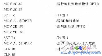
When reading data, T1 is set first, and the subsequent RD signal sends the row address to address line AB and makes D. The flip-flop latch Tl, Q, becomes low level, makes RAS active (low level), realizes row strobe; then sets TO to l, then the RD signal sends the column address to AB, and generates CAS The signal causes the data of the unit to be read to appear on the DB. The rising edge of the RD failure causes the CAS to fail. At the same time, the D2 flip-flop is set to 1, clearing D1 and RAS failing to high. After RC delay discharge, the data of the unit to be read appears on the DB, D2 is cleared again, and Q2 is high again, and the initial state D1 and D2 are zero.
At the end of the program, T0 and T1 are low-level, and RAS and CAS are blocked to prevent other reader/writer operations in the system from causing DRAM malfunction.
The process of writing data is similar.
2.54mm Pitch
2.54mm Pitch
ATKCONN ELECTRONICS CO., LTD , https://www.atkconn.com