When must the op amp be active?
problem:
Can I use the amplifier's disable pin to save power without affecting performance?
In the Internet of Things era, battery-powered applications are growing. This article will show that we don't have to make trade-offs between power savings and accuracy.
Some op amps have a disable pin that, if used properly, can save up to 99% in power consumption without compromising accuracy. The disable pin is primarily used for static operation (standby mode). In this mode, all ICs switch to a low-power state, eliminating the need to use a device to process the signal. This reduces power consumption by several orders of magnitude.
If the op amp needs to be used as a buffer amplifier for the ADC, as shown in Figure 1, it must be active to perform its function. However, if the amplifier is switched to the shutdown mode by disabling the pin, low power consumption can still be maintained. In general, the shutdown mode can be used as long as the ADC does not need to read any new values ​​into its sample and hold function blocks.
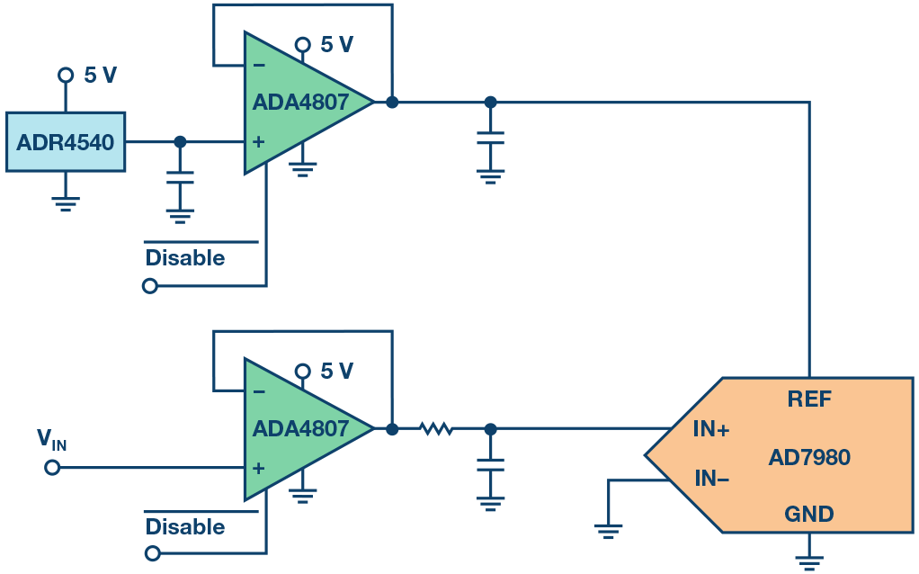
Figure 1. Typical schematic of an ADC input stage with an ADC driver and a reference buffer.
The easiest way to do this is by converting the start command. In a standard ADC, the input (sample-and-hold) capacitor is first charged to the value to be measured. This part is done before the signal is sent to the ADC for conversion. The input capacitor is then isolated and connected to the input of the converter stage, ie the conversion begins. The conversion is then complete and the completed signal is set, depending on the converter type. The real question now is: When must the op amp be active? The amplifier must operate ahead of the conversion start signal long enough to ensure that the internal input capacitor achieves the same value as the signal under test. The length of time depends on the size of the input capacitor, the amount of voltage to be measured, and the rate at which the op amp drives the capacitive load.
The ADC (AD7980) data sheet gives an input capacitance of 30pF when connected in series with 400 impedance. However, op amps are not that simple. The capacitive load listed in the parameter table is 15pF, but it is also possible to be higher, see the corresponding graph (Figure 2). Also consider the case where a low pass filter is used at 2.7nF and 20.
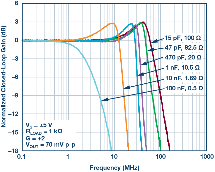
Figure 2. Frequency response of the ADA4807.
This graph shows that the module can drive a sufficiently high capacitive load. When disabled, the amplifier takes approximately 500ns to reach the full-scale output level, which in this case is 5V or 4.096V.
For the sake of safety, we assume that the amplifier is turned on 750ns before the start of the conversion. Compare the estimated data from 1kSPS to 1MSPS.
At 1kSPS, it is possible to save 99.83% of power (total power consumption of 0.02mW) and 92.41% of 1MSPS (total power consumption of 10.75mW). This is only the power savings of the ADC driver; the reference buffer also saves power.
This example is intended to illustrate the capabilities of modern devices. With a minimum sampling time of 500ns, the SINAD deviation is less than 0.5dB. For drives, you need to focus on faster, faster devices and use them flexibly. We only considered the application used as a buffer (gain = 1). For inverting or other amplifiers, power savings will vary from case to case. Need to be further analyzed by measurement.
Nlw-Ecl Pm Fiber,Diode Pumped Lasers,Gemini Diode Laser,Gp Fast Diode Laser
AcePhotonics Co.,Ltd. , https://www.acephotonics.com