Design of high precision sampling protection circuit for brushless DC motor
Summary
In this paper, a high-precision sampling and protection circuit is designed. This circuit can collect the three-phase current of the brushless DC motor in real time, so that the control system can perform closed-loop control and quickly protect the motor and control system. Finally, the experiment proves that the circuit has high precision and good reliability, which can effectively guarantee the normal operation of the control system and the motor.
In the brushless DC motor control system, the current sampling and protection circuit is used as a feedback link. The function is to detect and collect the current of the motor during real-time detection. After processing, the current signal is converted into a small voltage that can be recognized by the control system. Signals allow the control system to make appropriate control and protection actions. Since the motor current is an alternating current, the current sampling and protection circuit needs to have a rectifying function. The core component of the ordinary rectifying circuit is a diode with unidirectional conductivity, usually using one, two or four diodes to form a half-wave, full-wave Or bridge rectifier circuit. However, the diode exhibits nonlinearity in small signals, which will cause distortion of the rectified waveform (small signal portion). More seriously, the diode has a dead zone voltage. When the input signal is less than the deadband voltage, the diode does not. Turning on, thus causing severe distortion of the output signal, causing errors, such errors will not be negligible in small signals. In order to improve the accuracy, the amplification effect of the integrated op amp and the characteristics generated by the deep negative feedback are used to overcome the error caused by the nonlinearity of the diode. A high reliability and high precision sampling protection circuit is designed for a certain type of brushless DC motor. .
1 High precision half wave rectifier circuit
The rectifier circuit is a circuit that converts positive and negative alternating voltages into unipolar voltages. The half-wave high-precision rectifier circuit in this paper adds a diode to the proportional-amplifier circuit, and uses the unidirectional conductivity of the diode to introduce negative feedback with different depths in the positive and negative half cycles. The half-wave high-precision rectifier circuit constructed according to this idea is shown in Fig. 1.

Figure 1 Half-wave high-precision rectifier circuit
During ui "0" (0 to t1, t2 to t3). When the ui is still very small, both D1 and D2 are cut off, and the op amp is in an open loop state, and the open loop magnification is large. Therefore, ui only needs to be slightly larger, which makes u0' large enough and positive. As long as u0' is greater than 0.7 V, D1 is turned on and D2 is turned off (point a is zero potential), so D1 and Rf are connected in series with moderate negative feedback. The circuit at this time is equivalent to the inverting proportional amplifier circuit. The output is u0=-Rf/R1 * ui. The output u0 is proportional to the input ui, and u0 has the same shape as the waveform -ui, but is enlarged or reduced by a certain ratio. If R1=Rf, u0=-ui. From the above analysis, it is known that even if the input voltage ui is smaller than the initial on-voltage of the diode, the -Rf/R1 output is still present.
In ui "0 period (t1 ~ t2). When |ui| is still very small, both D1 and D2 are turned on. At this time, the op amp is in an open loop state, and its open loop amplification is large, so |ui| only needs to be slightly larger, and the op amp output u0' will It is large and negative, which causes diode D1 to turn off and D2 to turn on. The conduction of D2 introduces deep negative feedback to the op amp. Since the potential at point a is zero (virtual ground), u0'≈-0.7 V; and D1 is off, and the potential at point a is zero, so u0=0, that is, the u0 end wave has no waveform. The whole process is shown in Figure 2.
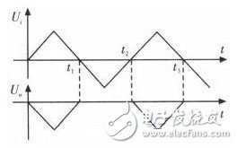
Figure 2 Half-wave rectification waveform
For example, if the frequency of the input signal is 50 Hz, the open-loop voltage amplification factor of the op amp is 5x10⁴, and the initial turn-on voltage of the diode is 0.5V, then the minimum rectified voltage (ie, the input signal) is only 10μA. That is to say, as long as the input signal is greater than 10 μA, the rectifier enters the normal working state; for the ordinary diode half-wave rectifier, the input voltage must be greater than 0.5 V (5 & TImes; 105 μV) to work properly, and the input voltage is 50,000 times that of the former. It can be seen that the circuit greatly improves the rectification accuracy. Figure 3 shows the transmission characteristics of the rectifier circuit, which is a straight line whose slope of origin is -Rf/R1.
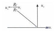
Figure 3 Transmission characteristics of the rectifier circuit
2 current sampling and protection circuit design
2.1 Hall sensor
The Hall current sensor is an advanced electrical detection component that isolates the main circuit and electronic control circuitry. It combines all the advantages of transformers and shunts while overcoming the deficiencies of transformers and shunts (the transformers are only suitable for 50 Hz power frequency measurements; the shunts are not capable of isolated measurements) and can measure the current of arbitrary waveforms. High precision, good dynamic performance, and wide frequency band. The Hall sensor in this paper uses lem LF205-S. The maximum current measurement range of this sensor is ±200 A, and the effective measurement range is ±100 A. When the measured current is in the effective range, the output voltage is: ±4 V, the measurement accuracy is 1%, the dynamic response time is less than 7 μs, and the tracking speed di/dt is higher than 50 A/μs.
2.2 TL082 Dual Operational Amplifier
The TL082 is a general purpose J-FET dual operational amplifier. Its characteristics are: low input bias and offset current; output with short circuit protection; input stage with high input impedance built-in frequency compensation circuit, in the current protection circuit design, use TL082 to form high-precision half-wave rectification Circuit and adder, and because TL082 is a dual operational amplifier, it saves space on the control board, making the design of the circuit more compact and compact.
2. 3 TL431 three-stage programmable shunt regulator diode
The TL431 is a three-terminal adjustable shunt reference source with good thermal stability. Its output voltage can be arbitrarily set to any value from Vref (2.5 V) to 36 V with two resistors (Figure 3). The device's typical dynamic impedance is 0.2 Ω, which can be used in many applications instead of a Zener diode. The output is a fixed voltage value. The formula is: Vout=(R1+R2)x2.5/R2
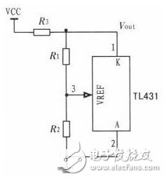
Figure 4 TL431 constant voltage 5V output circuit diagram
When R1 takes a value of 0, R2 can be omitted. In this paper, the constant current voltage source 5 V is used to supply power to the comparator.
Food Processor 10 In 1 is one of the most popular model among our Food Processors. They include almost all the features that can meet the needs of family life.
Description for Food Processor 10 In 1
400W
1.0L glass jar blender, grinder, juicer, citrus, juicer, mixer, meat mincer
2 speeds with pulse
shink bag packing
Color box: 66*24.5*44.5cm
40'HQ: 970pcs

Food Processor 10 In 1
Food Processor 7 In 1,Food Processor Blender Juicer,Electric Stainless Steel Food Processor,Electric Vegetable Food Processor
Flying Electronic Co., Ltd , https://www.flyingelectronic.com