A Design Scheme of Fingerprint Identification System Based on USB and DSP
Universal Serial Bus (USB) is a new type of interface technology. It is a serial communication standard developed by companies such as Intel and Microsoft to address the growing contradiction between peripherals and limited motherboard slots and ports. USB has the following features: (1) has a higher transmission rate. USBl.1 supports both full-speed and low-speed modes. The full-speed rate is 12Mbps and the low-speed rate is 1.5Mbps. In addition to the two speed modes of USBl.1, USB2.0 also increases the high-speed mode up to 480Mbps. (2) Easy to use and flexible. USB supports plug and play and hot swap, allowing peripherals to be connected and disconnected at any time. When a peripheral is connected, the system automatically detects the peripheral and is ready to use it. (3) Easy to expand. The root hub can carry 127 devices and truly realize that multiple peripherals share one interface. In addition, USB has the advantages of high reliability, low cost, and low power consumption.
1 overall program selection
Since the fingerprint image processing technology requires high real-time performance and large computational complexity, a general-purpose digital processing chip is adopted. DSP's high-speed computing performance makes it unique in the processing of digital signals. However, the amount of data of the digital signal is very large, and a convenient, high-speed interface is needed to realize the connection with the PC. This paper presents a low-cost high-speed USB interface solution based on DSP (TMS320VC5402) platform. It uses Philips' PDIUSBDl2 interface chip to realize DSP fingerprint image acquisition processing and high-speed data transmission of PC. The system covers digital image processing technology such as image acquisition, processing, storage and transmission. The hardware principle is shown in Figure 1.
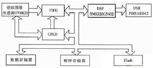
Figure 1 hardware block diagram
The fingerprint image and the digital output are obtained by the image sensor, and the image data is transmitted to the central processing chip DSP. The DSP performs real-time processing on the image, such as: filtering, smoothing and sharpening of the image, binarization, feature point extraction, etc., and the processing result is output to the host computer through the USB. In the whole fingerprint image acquisition and processing system, the DSP mainly has three functions: setting the contrast, brightness, sharpness and other parameters of the OV6620 through its I2C bus; digitally processing the fingerprint image; responding according to the USB specification, Provide device identification, solidify PDIUSBDl2, and communicate with the host computer.
2 system hardware program selection and design
2.1 Image sensor
CMOS image sensor is a new type of image sensor that has developed rapidly in recent years. It can integrate pixel array and peripheral support circuit on the same chip. It is a complete image system. Compared with CCD products, it has low power consumption, small size and low cost.
In the acquisition system, the OV6620 is used as an image acquisition chip. The OV6620 is a CMOS black and white image acquisition chip developed by Omni Vision. The chip integrates a CMOS optical sensing core with peripheral support circuitry. The output video is a black and white image. Technical parameters: resolution 352x288, speed 30 frames / sec.
2.2 Digital Signal Processing Chip
This system uses TI's high-performance digital signal processor TMS320VC5402. It adopts Harvard bus structure with completely independent program space and data space. The execution of instructions is pipelined. One or more processing cores are internal, with on-chip hardware multipliers. The instruction execution speed is up to tens of nanoseconds. It is 100 MIPS. These provide a broad application space for DSP in high-speed and large-data data acquisition and processing systems. There are 8 buses (4 program memory bus, 1 data memory bus and 3 address buses), on-chip memory and on-chip peripheral circuits. There is a highly specialized instruction system with low power consumption, high parallelism, etc. advantage.
2.3 USB interface chip
Many semiconductor companies in the world have participated in the development of USB chips and formed a variety of product lines. Such as Intel 8*930AX/HX, Cypress FX2 high-speed USB microcontroller, NaTIonal Semiconductor's USBN9602/9603. For the USB interface design based on DSP platform, after considering several options, it is decided to use a USB interface chip PDIUSBDl2 without MCU core, plus simple peripheral circuit and timing adjustment circuit. Mainly because it meets project performance requirements and uses an external CPU, the cost is very low.
PDIUSBDl2 is a prominent USB interface chip introduced by Philips. Fully compliant with the USBl.1 protocol, it integrates a serial interface engine (SIE), a 320-byte multi-structure FIFO memory, a transceiver (Transceiver), and a voltage regulator. It can operate at 5V or 3.3V operating voltage; has an 8-bit data bus and has a fully autonomous DMA transfer operation. It also has a controllable software connection (SoftConnect) function to ensure that the USB bus is connected after the microcontroller is reliably initialized. Multi-interrupt mode enables batch and isochronous transfers, enabling 1MB/S data transfer rates in both batch and sync modes. PDIUSBDl2 features high integration, high reliability and a wide range of operating conditions, making it easy to adapt to most DSP operating environments.
3 software design
3.1 Firmware Design
Firmware programming is an important part of the terminal device programming in the USB data transmission system. The microprocessor exchanges data with the computer through the firmware program. Since the USB interface chip without the MCU core is used, the implementation of the USBl.1 protocol specification must be completed by the DSP (TMS320VC5402) controlling the PDIUSBDl2 chip, and the program is written on the platform of the DSP (TMS320VC5402) to complete the USBl.1 specification. The required standard request and the user's own defined request according to the product.
When the device is connected to the host, the host sends a control transfer (ie, Setup package) containing the standard USB request to endpoint 0 of PDIUSBDl2. PDIUSBDl2 generates an interrupt to the MCU (1NT0). The MCU reads the interrupt register of PDIUSBD1 and the last transfer state. The register responds to each request and sends back the request message via endpoint 0 of PDIUSBDl2. The host reads the description data (including device descriptors, configuration descriptors, interface descriptors, endpoint descriptors, string descriptors) from the returned information, allocates and loads a device driver, and configures the device. Once the device is configured, you can transfer data using the endpoints supported in the configuration. The firmware program structure is shown in Figure 2.
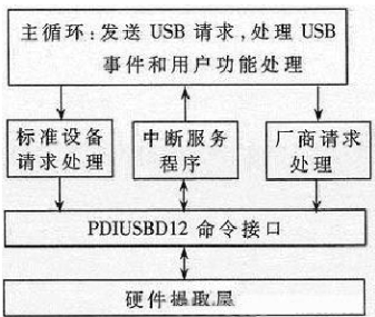
Figure 2 firmware program structure
3.2 device driver
3.2 device driver
In the Win32 system, each device is abstracted into a file. At this time, the application can communicate with a device in the driver by simply operating the AP1 function through a few simple files.
The driver for the PC is provided by Philips. Write a PC application by calling VC function with VC++6.0. In this way, the control of the DSP (TMS320VC5402) fingerprint imaging system and the image transmission can be realized by the PC. The main API functions used are DeviceIOControl(), ReadFile(), and WriteFile(). DeviceIOControl() is used by the PC (host) to send requests to the DSP image acquisition system; ReadFile() and WriteFile() are used to read data from the image acquisition system and write data to the image acquisition system, respectively. The problem that must be paid attention to during the design process is that since the USB interface is the master-slave interface, all transmission processes must be started after the host sends a request to the peripheral, so read and write using ReadFile() and WriteFile(). Before the data, the request must be sent to the image acquisition system via DeviceIOControl().
3.3 Fingerprint Identification Process
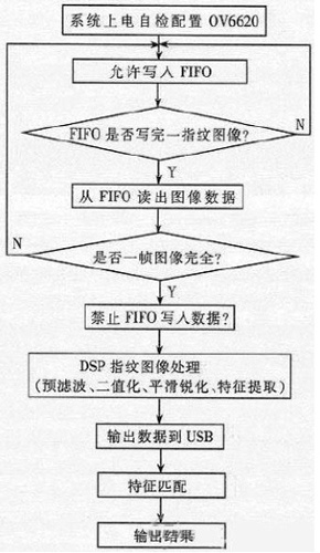
When the system is powered on, the TMS320VC5402 sets the OV6620 through the 12C bus operation and then enters the fingerprint image acquisition phase. At this stage, the TMS320VC5402 is in an idle state, and the CPLD occupies the data bus.
Store data directly into the image RAM. After collecting one frame of fingerprint image, the CPLD sends a handshake signal to inform the DSP to enter the data processing stage. At this stage, the TMS320VC5402 first transfers the data in the image RAM to the user RAM, performs image preprocessing, feature point extraction, etc., and finally outputs the result to the host computer via USB. The upper computer calls up the fingerprint database, and compares the extracted result with the data in the fingerprint feature database to perform fingerprint matching identification with the feature fingerprint in the library.
The DSP algorithm is as follows: (1) Pre-filtering. Directional filtering: A horizontal template is designed, and then the horizontal template is rotated to the direction of the desired enhancement for filtering. (2) Binarization. Background separation: Using the standard deviation threshold tracking method, the fingerprint part of the image is composed of black and white textures. The gray scale varies greatly and has a large standard deviation, while the gray part distribution of the background part is relatively flat and the standard deviation is small. Therefore, the standard deviation of a group of pixels centered on each point is calculated. When the standard deviation is greater than a certain threshold, the point can be determined as the foreground, otherwise it is the background. (3) Computational direction map: A method based on the normal vector is used, which also involves the smoothing of the direction field. (4) Feature point extraction: The ridge line tracking method is adopted. The basic idea is to directly traverse the image and detect the feature points during the tracking process.
The entire software process is shown in Figure 3.
Cosmetic Instrument Vibration Motor Mainly used in cosmetic instrument, such as instrument, cleansing essence introducing vibration meter, wash a face, facial massage, hairdressing instrument, etc.


Operating temperature range:
Cosmetic Instrument Vibration Motor should be used at a temperature of -10~60℃.
The figures stated in the catalog specifications are based on use at ordinary room temperature catalog specifications re based on use at ordinary room temperature (approximately20~25℃.
If a Cosmetic Instrument Vibration Motoris used outside the prescribed temperature range,the grease on the gearhead area will become unable to function normally and the motor will become unable to start.Depending on the temperature conditions ,it may be possible to deal with them by changing the grease of the motor's parts.Please feel free to consult with us about this.
Storage temperature range:
Cosmetic Instrument Vibration Motor should be stored ta a temperature of -15~65℃.
In case of storage outside this range,the grease on the gearhead area will become unable to function normally and the motor will become unable to start.
Service life:
â—Use with a load that exceeds the rated torque
â—Frequent starting
â—Momentary reversals of turning direction
â—Impact loads
â—Long-term continuous operation
â—Forced turning using the output shaft
â—Use in which the permitted overhang load or the permitted thrust load is exceeded
â—A pulse drive ,e.g.,a short break,counter electromotive force,PWM control
â—Use of a voltage that is nonstandard as regards the rated voltage
â—Use outside the prescribed temperature or relative-humidity range,or in a special environment.
â—Please consult with us about these or any other conditions of use that may apply,so that we can be sure that you select the most appropriate model.
when it come to volume production,we're a major player as well .each month,we rurn out 600000 units,all of which are compliant with the rohs directive.Have any questions or special needed, please contact us, we have the engineer group and best sales department to service to you Looking forward to your inquiry. Welcome to our factory.

Cosmetic Instrument Vibration Motor
Cosmetic Instrument Vibration Motor,Face Brush Vibration Motor,Electric Cosmetic Instrument Vibration Motor,Cosmetic Instrument Mini Vibration Motor
Shenzhen Shunchang Motor Co., LTD. , https://www.scgearmotor.com