MOSFET and MOSFET drive circuit principle and application
The following is a summary of my MOSFET and MOSFET driver circuit foundation, which refers to some of the information, not all original. Includes introductions, features, drivers, and application circuits for MOSFETs.
This article refers to the address: http://
When designing a switching power supply or a motor driving circuit using a MOS tube, most people will consider the on-resistance of the MOS, the maximum voltage, the maximum current, etc., and many people only consider these factors. Such a circuit may work, but it is not excellent, and it is not allowed as a formal product design.
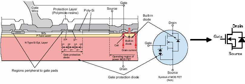
1, MOS tube type and structure MOSFET tube is a kind of FET (the other is JFET), can be made into enhanced or depletion type, P-channel or N-channel a total of 4 types, but the actual application is only Enhanced N-channel MOS transistors and enhanced P-channel MOS transistors, so NMOS is usually mentioned, or PMOS refers to both. The figure on the right is the symbol for these two MOS tubes.

As for why not use a depletion type MOS tube, it is not recommended to ask the bottom.
For these two enhanced MOS transistors, the NMOS is more commonly used. The reason is that the on-resistance is small and easy to manufacture. Therefore, in switching power supply and motor driven applications, NMOS is generally used. In the following introduction, NMOS is mostly used.
As you can see on the MOSFET schematic, there is a parasitic diode between the drain and the source. This is called a body diode, which is important for driving inductive loads such as motors. Incidentally, the body diodes are only present in a single MOS transistor and are usually not available inside the integrated circuit chip. The figure below shows the structure of the MOS tube. The normal schematic is drawn as shown on the right. (The gate protection diode is sometimes not drawn)
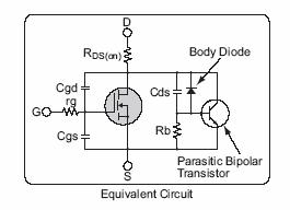
There is a parasitic capacitance between the three pins of the MOS transistor, as shown in the right figure. This is not what we need, but because of manufacturing process limitations. The existence of parasitic capacitance makes it more troublesome when designing or selecting the driving circuit, but there is no way to avoid it. It will be introduced in detail when designing the driving circuit of the MOS tube.
2, MOS tube conduction characteristics conduction means as a switch, equivalent to the switch closure.
The characteristics of the NMOS, Vgs greater than a certain value will be turned on, suitable for the case when the source is grounded (low-side drive), as long as the gate voltage reaches 4V or 10V.
The characteristics of the PMOS, when Vgs is less than a certain value, will be turned on, and when the VCC is connected to the source (high-end drive). However, although PMOS can be conveniently used as a high-side driver, NMOS is usually used in high-end driving because of high on-resistance, high price, and low replacement.
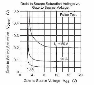
The picture on the right is a plot of Vsa voltage and Vds voltage for Renesas 2SK3418. It can be seen that when the current is small, the Vgs reaches 4V, and the voltage drop between the DSs is already small, which can be considered as conduction.
3, MOS switch tube loss, whether it is NMOS or PMOS, there is an on-resistance after conduction, so there will be voltage at both ends while flowing current between DS (such as 2SK3418 characteristic diagram), so the current Energy is consumed on this resistor, and this part of the energy consumed is called conduction loss. Selecting a MOS transistor with a small on-resistance reduces the conduction loss. The current low-power MOS tube on-resistance is generally in the range of several tens of milliohms, and several milliohms are also available.
When MOS is turned on and off, it must not be completed in an instant. The voltage across the MOS has a falling process, and the current flowing through has a rising process. During this time, the loss of the MOS tube is the product of voltage and current, called switching loss. Usually the switching loss is much larger than the conduction loss, and the faster the switching frequency, the greater the loss.
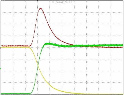
The figure below shows the waveform when the MOS transistor is turned on. It can be seen that the product of the voltage and current at the turn-on instant is large, and the loss is large. By reducing the switching time, the loss per turn-on can be reduced; reducing the switching frequency can reduce the number of switches per unit time. Both of these methods can reduce switching losses.
4, MOS tube drive compared with bipolar transistors, it is generally considered that the MOS tube does not require current, as long as the GS voltage is higher than a certain value, it can be. This is easy to do, but we still need speed.
It can be seen in the structure of the MOS transistor that there is a parasitic capacitance between GS and GD, and the driving of the MOS transistor is actually charging and discharging the capacitor. The charging of the capacitor requires a current, because the capacitor can be regarded as a short circuit when charging the capacitor, so the instantaneous current will be relatively large. The first thing to note when selecting/designing a MOS tube driver is the amount of transient short-circuit current available.
The second note is that NMOS, which is commonly used for high-side driving, needs to have a gate voltage greater than the source voltage when turned on. When the high-side driving MOS transistor is turned on, the source voltage is the same as the drain voltage (VCC), so the gate voltage is 4V or 10V larger than VCC. If you want to get a voltage larger than VCC in the same system, you need a special boost circuit. Many motor drivers have integrated charge pumps. It is important to note that a suitable external capacitor should be selected to get enough short-circuit current to drive the MOSFET.
The 4V or 10V mentioned above is the conduction voltage of the commonly used MOS tube, and it is of course necessary to have a certain margin when designing. Moreover, the higher the voltage, the faster the conduction speed and the smaller the on-resistance. There are also MOS tubes with smaller turn-on voltages used in different fields, but in 12V automotive electronic systems, 4V turn-on is generally sufficient.
For the drive circuit of MOS transistors and their losses, refer to Microchip's AN799 Matching MOSFET Drivers to MOSFETs. The story is very detailed, so I don't plan to write more.
5, MOS tube application circuit MOS tube's most remarkable feature is the good switching characteristics, so it is widely used in circuits that require electronic switches, such as switching power supplies and motor drives, as well as lighting dimming. These three applications are described in detail in various fields, and there is not much to write here. I will have time to summarize later.
LED Street Lights,Street Lamp,LED Street Lamp
LED Bulb Light Bracket Co., Ltd. , http://www.challleds.com