Research on Smart Home Control System Based on GSM Short Message
1 Introduction
At present, a large number of household electrical appliances are used in people's home life, but these household electrical appliances require people to directly control them. Although they can be controlled with some timing, they have limited functions and poor flexibility. As mobile phones are becoming more and more popular as mobile terminals, developing their extended applications will have a broad base of equipment and broad market prospects. You can use mobile terminals to rely on the public information network to control home appliances and query home conditions. This article discusses an attempt to combine information processing technology and device control to realize digital home, so that people can enjoy the convenience brought by the information revolution to life. The innovation of this article is to use ZigBee technology for home networking, combining DSP technology and SMS to complete the communication between remote devices and users. In this way, the network coverage is wide, and the advantages of no dialing, low price, and wide coverage are required for control and monitoring, and there is no need to re-arrange the power grid.
2 System hardware design
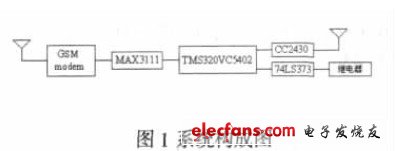
The smart home system has the functions of remote control, remote query, and centralized management of various devices in the home, providing users with a more comfortable and convenient lifestyle. This design is mainly aimed at home appliance control. The ZigBee communication sub-node needs to have functions such as pulse data collection, switch data collection, analog data collection, and relay contact output. The master node is actually a fully functional FFD device, which manages the home subnet node, and Communicate with the home server to realize the information interaction between the server and the child nodes. In this design, the internal node of the home is mainly composed of the radio frequency chip CC2430 and the TMS320VC5402 chip. CC2430 is a ZigBee wireless network module that complies with the IEEE802.15.4 standard (MAC, and PHY layer). The TMS320VC5402 chip is used to control the operation of the CC2430ZigBee module, and is connected to the GSM module through the MAX3111 for data communication. We integrated ZigBee's coordinator node and GSM module into one board. The node is in a sleep state during idle time. When the user has a control signal or data collection request, an interrupt is used to wake up the node, complete the data collection or control task, and report related information.
The system configuration diagram is as follows:
The main control center module is responsible for receiving the short message, judging the command, issuing the command or directly driving, and sending the working state of the machine to the mobile terminal by short message.
This kind of work can choose low-cost ordinary C51 single-chip microcomputer. But consider to expand the application of image-based MMS feedback in the future, so in this design, the processor of the controller chose the TMS320VC5402 chip. DSP main control module uses TMS320VC5402EVM evaluation board and emulator. TMS320VC5402EVM provides two BCMSP direct connection ports J6, J7 and PHI driver ports J2 and J5 to connect with the emulator. The board has 512KRAM data storage, 64KRAM as program storage. 4KFLASH memory can be used to store the data to be retained.
To connect TMS320VC5402 to the GSM module, the RS232 interface needs to be expanded. TMS320VC5402 only provides two multi-channel buffered synchronous serial ports MCBSP0, MCBSP1. If docking is achieved, the MCBSP serial port must be converted. We are using the MAX3111 chip here. The MAX3111 chip has the characteristics of small size, low price, low power consumption and high communication rate. Use MAX3111 chip to realize the conversion from synchronous serial data interface to asynchronous serial port (RS-232). It can be connected to the RS232 port of H6221. The MAX3111 includes two parts: UART and RS-232. The UART part includes SPI compatible serial port, programmable baud rate generator, transmit buffer and transmit shift register, receive buffer, receive shift register, 8 words Section receive FIFO, and there are four kinds of interrupt generators that can shield the interrupt source. The RS232 part includes an electric pump with its own capacitor.
Because the MAX3111 is a 3.3V device, the MCBSP serial interface of the TMS320VC5402 can be directly connected to the MAX3111 to implement asynchronous data transmission with RS232 devices when working in SPI mode. At this time, TMS320VC5402 is the master device in the SQI protocol, sending the time-resolving signal (BCLKX) as the MAX3111 serial time-resolving input, and sending the frame synchronization signal (BFSX) as the MAX3111 original selection signal (TCS). BDX and DIN are connected as the sending data line. BDR and DOUT are used as receiving data lines.
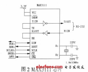
The function of MAX3111 can be customized by sending 16-bit control word configuration commands to it through the BDX line. The MAX3111's TX is connected to T1IN, and RX is connected to R1OUT to use its on-chip converter to achieve UART to RS232 level conversion.
The MAX3111 serial interrupt signal (IRQ) is connected to the DSP's external interrupt LNTO. This does not require any other peripheral devices. Since the asynchronous transceiver is implemented by the MAX3111 hardware, the software programming of the TMS320VC5402 only needs to consider the synchronous data communication with the MAX3111.
The connection between TMS320VC5402 and CC2430 is the execution link of the system. Because CC2430 is C51 as the core, the connection between TMS320VC5402 and CC2403 is similar to the connection with C51 microcontroller, but the level of CC2430 is 2-3.9 volts.
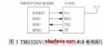
The TMS320VC5402 interface level is 3.3 volts, which can be directly matched, reducing the trouble of level conversion.
When the execution terminal receives the call to the machine and confirms the execution command issued by the center, it drives the output pin of the corresponding port. As shown in the figure above, P0.0 drives the transistor Q, driving the relay J0, and the three normally open contacts are closed, J0. Lesson 1 drives the load, and J0.2 is detected by P1.0, and the status of J0 is available for query.
Waterproof Speaker,Full Range Loud Speaker,Entrance System Speaker,Waterproof Multimedia Speaker
Jiangsu Huawha Electronices Co.,Ltd , https://www.hnbuzzer.com