Implementation of HDLC to E1 transmission controller based on FPGA
Abstract: This article introduces an FPGA-based HDLC to E1 protocol controller, which can realize the transfer of HDLC data with a rate of N & TImes; 64Kbps (N = 1 ~ 124) to M channels (M = 1 ~ 4) E1 Transmit in the channel, and allow the maximum delay of each channel E1 to be 64ms. The E1 frame structure design and FPGA implementation method of the system are discussed.

introduction
E1 is the transmission standard used by the primary group of China's telecommunications transmission network. Because China's E1 resources are very rich, such transmission paths are very easy to obtain. Flexible use of the existing abundant E1 channels to transmit HDLC data can save a lot of transmission costs. Generally, one HDLC data is transmitted through only one E1 channel, but if the rate of HDLC data is large and the bandwidth of one E1 signal is not enough to transmit, then HDLC data will be distributed to the M E1 channel for transmission, and the receiving end The HDL data is recovered by combining the E1 signals of the channels. If the transmission paths of the M channel E1 signals are different, it will definitely cause different delays. When this system is designed, the maximum delay of each E1 signal is allowed to be 64ms.
System E1 frame structure design The frame structure of the E1 stream in this system can be obtained by referring to the PCM group 30/32 channel system frame structure proposed by CCITT G.732, G.704 or G.706, but it is different .
The composition of information bits The payload (information bits) to be transmitted by this system is N & TImes; 64Kbps HDLC data. TS16 signaling time slot in standard E1 and 31 time slots TS1 ~ TS15 and TS17 ~ TS31 can transmit the payload. Therefore, N and M satisfy the relationship N≤31 & TImes; M. For the maximum case, namely N = 124 and M = 4, the net load occupies 31 time slots. When N <124, so that all 31 time slots cannot be filled, the invalid bit '1' is fixed.
The design of the TS0 time slot takes into account that the system must be able to realize the independent transmission of one N & TImes; 64Kbps HDLC data in the M channel E1 channel by bit, and correctly recover this data at the receiving end through the combination. The combination process requires M The E1 signal of the channel is completely synchronized, and there are different degrees of delay between the channels in the actual line, which requires the system to have a delay buffer capacity. During this period, a memory is used to buffer the data. In order to distinguish the CRC multiframe stored in SRAM in a certain way, it should be combined with the corresponding CRC multiframe stored in SRAM in other ways, that is, in order to achieve multiframe synchronization, each CRC multiframe needs to be labeled, that is, Add multi-frame positioning code. In addition, since HDLC data is transmitted in M ​​channels of E1 channels by bit tapping, when M = 2, 3, 4, then the information bits in M ​​channels of E1 channels must be received at the receiving end in the order of tapping at the time of transmission. Multiplexed into HDLC data by bit. Therefore, each way E1 needs a way label representing the order of multiplex / multiplex. In order to make full use of E1 channel resources, the three spare bits after the E1 odd frame header are used to provide users with a 12Kbps synchronous data channel, which can also be used as a low-speed asynchronous data channel, such as the commonly used 2400, 4800, 9600bps RS-232 signals .
System design Hardware design The hardware part of the system includes an FPGA and an SRAM. FPGA uses Altera's Cyclone series EP1C6. Cyclone series devices are low-cost, medium-density FPGAs, with 5980 logic cells inside, 20 4Kbit RAM blocks, and 2 internal phase-locked loops.
Since the system allows each E1 channel to have a maximum delay of 64ms, a multiframe period is 2ms, that is, the maximum delay is 32 multiframe times. A multi-frame consists of 16 basic frames, and the number of bits of 32 multi-frames is 32 × 256 × 16 = 128Kbit, then the maximum capacity of RAM required by each channel is 128Kbit. Since the maximum number of channels M = 4, the maximum RAM capacity required by the system is 4 × 128Kbit = 512Kbit. The EP1C6 only has 80Kbit of RAM, so choose the method of using external RAM. This system uses Inbond's W24L01 with a capacity of 1024Kbit.
Realizing system functions through VHDL The system uses a top-down EDA design process and uses VHDL language programming to achieve system functions.
The sending part is mainly composed of phase-locked loop module, shunt module, framing module, CRC check module and serial scrambling module. In the main clock mode, the local crystal oscillator generates N × 64KHz clock and 2.048MHz clock through rational number frequency division. The N × 64KHz clock is used as the clock generation source of HDLC data. N × 64Kbps HDLC undergoes serial / parallel conversion and writes to M buffers, then read it with the 2.048MHz clock, and insert it into the corresponding time slot of the E1 frame to form the M E1 signal, which is checked by CRC-4, and finally sent through the serial scrambling code. . In the slave clock mode, the N × 64KHz clock is provided by HDLC, and the 2.048MHz clock is extracted from the N × 64Kbps HDLC by the phase-locked loop module. The selection of clock mode and the values ​​of M and N can be programmed through VHDL language within the FPGA.
The receiving part includes a phase-locking module, a frame header detection module, a descrambling code module, a read-write RAM module, and a combining module. In the receiving part, first use the phase-locked loop to lock out the 2.048MHz synchronization clock and N × 64KHz clock through the input E1 signal, and use the 2.048MHz clock to detect the frame header of the E1 signal. After the frame header is found, the system enters the frame synchronization state , And then descramble the code, CRC reverse check, and extract other various control information and data. The data after descrambling code is output to FPGA after serial / parallel conversion and stored in off-chip RAM. After receiving the control information, FPGA starts to read data from RAM, and performs parallel / serial conversion under the control of N × 64KHz clock, removes the frame header, and finally synthesizes an N × 64Kbps HDLC output signal.
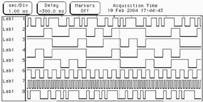
Figure 1 Simulation waveform diagram Simulation and test The entire system and each sub-module are functionally simulated and post-simulated. The functional simulation platform is ModelSim + 5.5f, the integrated platform is FPGA Express 3.5, and the post-simulation platform is Altera Quartus 3.0. The measured waveform with the logic analyzer HP54645D is shown in Figure 1 (take M = 4, N = 104).
Conclusion Through VHDL programming of FPGA, the HDLC data with a rate of N × 64Kbps (N = 1 ~ 124) is tapped into the M channel (M = 1 ~ 4) E1 channel for transmission, and the E1 odd is fully utilized The TS0 time slot of the frame provides users with a synchronous data transmission channel of 12Kbps, and allows E1 to have a delay of 64ms. The HDLC to E1 transmission controller designed in this paper can also be used as a transition bridge for other protocol converters. For example, the 10Base-T Ethernet signal can be transferred to the HDLC protocol controller (such as the ADM6993 chip produced by ADMtek), and then transferred to the E1 transmission controller through HDLC, thereby realizing the function of Ethernet over TDM.
Advantages of Solar Flood Lights
1. Electricity and money economy On of main advantages for using LED solar flood lights is efficiency and power economy. They have a solar panel set with LED light that accumulates solar energy on what light can be powered whenever needed. Running on solar energy means that you do not have to pay anyone for electrical power, solar energy is free for everyone. This means saving up money and cutting on electrical bills.
2. Can work in places and areas with no reachable electrical power Other advantage of solar lights is that they can be used in areas where other electrical source to power light can not be reachable. This can be good for outdoor places like gardens, backyards or sheds, or other places without electricity. At home a nice option would be to use LED solar flood light as a front door or garage light combined together with motion detector to save up more energy and provide longer work time with one charge at time.
3. Using alternative energy – environment friendly Even if you are not all into green lifestyle, it is good to consider a little bit about environment around you. And solar lights are one of many things, that can actually help environment by using alternative energy. It may not sound interesting, but it is certainly an advantage for solar lighting and green thinking.
Solar Flood Lights
Solar Flood Lights,Solar Flood Light With Camera,Solar Flood Light For Flagpole,Solar Flood Light Motion Detector Weatherproof
Jiangmen Biaosheng Solar Energy Technology Co., Ltd. , https://www.bsprosolar.com