General intelligent wireless transceiver device based on nRF401
General intelligent wireless transceiver device based on nRF401
At present, wireless data transmission devices need to be embedded in various instrumentation data collection systems and remote control measurement and control systems.This paper introduces a design method and hardware for a universal wireless transceiver device that intelligently controls the wireless transceiver chip nrf401 through the single chip microcomputer w77e58 The design of the circuit is divided into two parts: the design of the radio frequency module and the design of the control module. The device can select the serial port as rs232 standard or ttl level standard through the jumper device. The w77e58 control can realize dual channel switching and data flow control.
1 Design of wireless radio frequency module
In this design, the radio frequency module uses the nrf401 wireless transceiver chip launched by Norwegian nordic company. The chip uses the 433mhz ism frequency band and is a true single-chip uhf wireless transceiver integrated chip.In a 20-pin chip, it includes high-frequency transmission, high-frequency reception, pll synthesis, fsk modulation, fsk demodulation, multi-channel switching, etc. , Is currently the most integrated wireless data transmission product [1]. The radio frequency module uses an on-board differential loop antenna. The load impedance of the antenna port is 380ω. The circuit principle is shown in Figure 1. The parameters of each peripheral component are listed in the figure. Among them, the j1 port is the interface between the radio frequency module and the control module.
The design points of the hardware circuit are as follows:
(1) The RF circuit is quite sensitive to power supply noise, and the star wiring method must be used to make the digital part and the rf part have their own power lines, and should be decoupled near the power supply pins of the integrated circuit [2].
(2) High-frequency inductance is selected for external vco electric induction, q> 45, accuracy is 2%, this design uses lqw18an22ng00 of Shenzhen Shunbai Technology Co., Ltd. The accuracy of the inductance has a greater impact on the distance of wireless communication, and can also be used The accuracy is 5%, but the communication distance will be greatly reduced. The vco inductance connection should be kept at a certain distance from other control lines, the digital control line should be avoided from passing between the inductance pins, and the center of the vco inductance element should be about 5.4mm away from the center of the ncof401 vco1, vco2 pin pad The selection and layout of inductive components are very important, and they are the key to the success of the design.
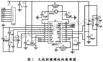
(3) A large area of ​​copper is used as the ground plane on both the front and back sides of the circuit board to make all devices easy to decouple. The copper on both sides should be connected using multiple vias. All connections to the ground layer must be as short as possible. The ground via should be placed very close to the pad of the component [2].
(4) The design of the antenna uses the loop antenna of the PCB board, the size is 35mm × 20mm, the antenna gain is -11db, the antenna impedance is 380ω, the antenna should be located on the top of the PCB board, and the antenna part should not be covered with copper. The design of the loop antenna can be Refer to nordic's technical documents nan440-03 and nan400-05.
(5) If the vco inductance of the pcb board is designed reasonably, when the module is in the receiving state, the voltage of the fourth pin of nrf401 is 1.1 ± 0.2v.
2 Design of control module
The control module is responsible for the control of the state switching and channel switching of the radio frequency module. The Winbond microcontroller w77e58 is selected. The design of the control module is divided into hardware circuit design and software design.
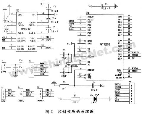
2.1 Design of hardware circuit
w77e58 has high speed, the working frequency can be extended to 40mhz, the same crystal oscillator running time as 8051/52 is 2.5 times faster than 8052 [3], and it has two uart serial ports on-chip, and serial port 0 is used for external serial device Communication, serial port 1 is used to communicate with the wireless transceiver module, of which j6 port is the interface between the control module and the wireless radio frequency module, and j2 port is the interface for the control module to communicate with external serial devices.You can use a simple three-wire communication method, or you can add the The control signal cts can reset the intelligent wireless data transmission module through the control of the reset pin through the ttl level. The j2 port and the external serial device can communicate in the form of rs232 or ttl level.The choice of communication mode is set by the jumper of the interface j3, j4, j5, and the max232 and peripheral capacitive components can all use chip devices to reduce pcb board space. Through p2.5, p2.6, p2.7, respectively control the switching of the standby state and the working state of the radio frequency module, the switching of the receiving and sending state, and the switching of the channel.
2.2 Software design
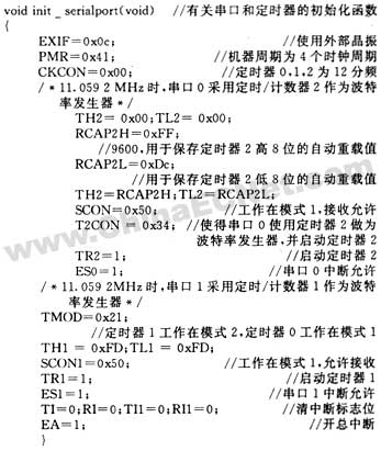
w77e58 comes with two serial ports, of which serial port 0 can use timer t1 or timer t2 as a baud rate generator; serial port 1 can only use timer t1 as its baud rate generator [4]. In this design, t2 is used as the baud rate generator of serial port 0, and t1 is used as the baud rate generator of serial port 1. Both serial ports work in serial port mode 1, the baud rate is 9600b / s, and serial port 0 is occupied When the No. 4 interrupt is used, scon and sbuf are used as its serial control registers and serial data buffers; serial port 1 occupies the No. 7 interrupt, and scon1 and sbuf1 are used as its serial control registers and serial data buffers. The initialization function for the serial port is init_serialport (), the function is defined as follows:
In the process of wireless communication, due to the interference of the external environment, the bit error rate is usually relatively high, even if the transmitter does not send data, the receiver will still often receive messy data due to external interference, in order to distinguish in the process of receiving Whether the received data is valid data, there must be a certain communication protocol:
(1) The data transmission of the two serial ports uses the query mode, and the data reception uses the interrupt mode;
(2) The data frame includes two parts: the frame head and the data. The frame head uses double bytes 0x55aa, the data part is 1b, that is, each frame occupies 3b, and the frame head and data part are transmitted in hexadecimal ascii code to ensure Transparency;
(3) If the receiver receives 0x55 0xaa bytes, it means that a valid data frame has been received, otherwise the frame is discarded.
If the hardware circuit design is reasonable, the selection of components is appropriate, and the above simple communication protocol, the bit error rate can be controlled below 0.2%.
After the single chip microcomputer is powered on, the system and the serial port are initialized first, and then the single chip microcomputer enters the standby mode until one of the two serial ports is interrupted and hard-switched to the working mode to handle the interrupt program. The main program code is as follows:

3 Testing of hardware circuits
In this design, the control module and the wireless RF mode are designed separately. The control module controls the RF module through a single row of 7-pin interfaces. The test steps are as follows:
(1) Weld the control module and the radio frequency module well, check and confirm that there is no virtual welding or stick welding;
(2) First test the power of the control module, mainly to test whether the serial port 0 and serial port 1 of the control module can send and receive data with each other. The test method is to set the serial port 0 to the rs232 standard through the jumper on the board. 1 There is only ttl level standard, you must add a level conversion circuit to convert it to rs232 standard, and then connect the two serial ports to the two serial ports of the computer, write the above program to w77e58, and then use the serial port test software to test , If the serial ports 0 and 1 can send and receive data to each other, you can start testing the wireless radio frequency module;
(3) Weld the j1 port of the radio frequency module and the j6 port of the control module, and test the power. According to the above procedure, the power is in the receiving state. You can test the pins such as txen, pwup, cs, etc. Whether it is consistent with the program;
(4) After confirming that the RF module is powered on and receiving, you can test whether the fourth pin of nrf401 is about 1.1v. If it is, it indicates that the vco inductance design is reasonable, otherwise the PCB board must be redesigned. In addition, nrf401 has no data. When receiving, random data will still be automatically sent from dout, and the voltage of this pin should be around 2.5v when using a multimeter for testing [4]. If you have an oscilloscope, you can do more detailed tests.
4 Conclusion
It consists of a wireless transceiver chip nrf401, a single chip microcomputer w77e58, an interface chip max323, etc., which constitutes an intelligent control wireless transceiver device, which is versatile and can be embedded in various instrumentation data collection systems and remote control telemetry systems to achieve two-way transmission of wireless data .
Breaker Mcb,Mcb Circuit Breaker,32A Circuit Breaker,Miniature Circuit Breaker
ZHEJIANG QIANNA ELECTRIC CO.,LTD , https://www.traner-elec.com