The chip manufacturing process is really difficult, it is easy to get it in seven steps!
The chip is not grown naturally, nor is it printed by a otaku with a computer. Its birth is a long and complicated journey. In simple terms, the chip manufacturing process has several stages: material preparation - monocrystalline silicon fabrication → wafer generation chip front end - wafer construction (Wafer Fabrication)
Chip backend - Package → Initial Test (Initial Test and Final Test)
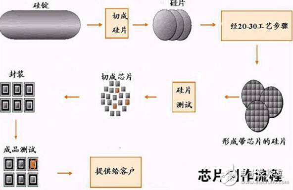
Preparation - Silicon wafer fabrication is inseparable from silicon. As the most important raw material, silicon processing is crucial. First, the silicon raw material is subjected to chemical purification, which is a step to achieve the level of raw materials available to the semiconductor industry. In order for these silicon raw materials to meet the processing needs of integrated circuit manufacturing, they must also be shaped by melting the silicon raw material and then injecting the liquid silicon into a large high-temperature quartz container.
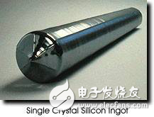
Then, the raw material is melted at a high temperature, and then the silicon raw material is taken out by a rotary stretching method from a high temperature container, at which time a cylindrical silicon single crystal ingot is produced. Currently, the industry's most advanced process produces 300mm silicon ingots, which are 12-inch wafers.
After making the ingot and ensuring it is an absolute cylinder, the next step is to slice the cylindrical ingot. The thinner the slice, the more material you use, the more processor chips you can produce. The slicing is also mirror finished to ensure that the surface is absolutely smooth and then checked for distortion or other problems. This step of quality inspection is particularly important, it directly determines the quality of the finished chip.
Some new materials are incorporated into the new slice to make it a true semiconductor material, and then trace the circuit that represents the various logic functions. The doped substance atoms enter the gap between the silicon atoms, and an atomic force acts between them, so that the silicon raw material has semiconductor characteristics. Today's semiconductor manufacturing is dominated by CMOS processes (complementary metal oxide semiconductors). Among them, the word complementary means the interaction between the N-type MOS transistor and the P-type MOS transistor in the semiconductor. N and P represent the negative electrode and the positive electrode, respectively, in the electronic process. In most cases, the slice is doped with a chemical to form a P-type substrate, and the logic circuit on which it is scribed is designed to follow the characteristics of the nMOS circuit. This type of transistor has higher space utilization and is more energy efficient. At the same time, in most cases, the presence of pMOS transistors must be limited as much as possible, because in the later stages of the manufacturing process, N-type materials need to be implanted into the P-type substrate, which leads to the formation of pMOS transistors.
After the work of incorporating the chemical is completed, the standard section is completed. Then, each slice was placed in a high temperature furnace and heated to control the heating time to form a silicon dioxide film on the surface of the slice. The thickness of the silica layer is controllable by closely monitoring the temperature, air composition and warming time. The final step in the preparation is to cover the silicon dioxide layer with a photosensitive layer. This layer of material is used for other control applications in the same layer. This material has a good sensitizing effect when dried, and can be chemically dissolved and removed after the photolithography process is completed. Photolithography
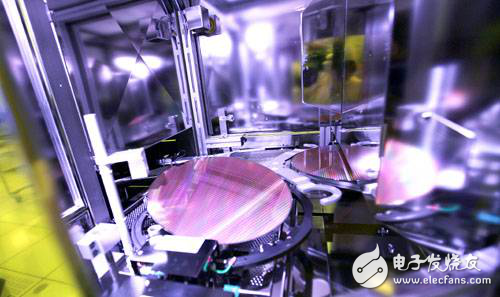
Lithography is the process of printing chip circuit patterns on a wafer. It is the most critical step in the fabrication of integrated circuits, accounting for about 35% of the overall manufacturing cost in the entire chip manufacturing process.
Lithography is also an important reason for the development of integrated circuits in accordance with Moore's Law. Without the advancement of lithography, integrated circuits cannot enter deep micron micron and then enter the nano era.
The photolithography process transfers the mask pattern onto the photoresist on the surface of the wafer. First, the photoresist processing device spins the photoresist onto the surface of the wafer, and after repeated exposure and development processes, forms on the wafer. The graphics you need.
It is usually difficult to represent the process by the number of masks required for a process. According to different exposure modes, lithography can be divided into contact type, proximity type and projection type; according to the number of lithography, there are single-sided alignment lithography and double-sided alignment lithography; depending on the type of photoresist, there are Thin film lithography and thick film lithography. The general lithography process includes pre-treatment, homogenization, pre-baking, alignment exposure, development, and post-baking. The operation in the process can be adjusted according to actual conditions.
Etching
In the manufacturing process of the integrated circuit, after mask registration, exposure and development, the desired pattern is copied on the resist film, or the electron beam is directly drawn on the resist film to produce a pattern, and then the pattern is accurately The transfer is carried out to a dielectric film (such as silicon oxide, silicon nitride, polysilicon) or a metal film under the resist to produce a desired thin layer pattern.
Etching is the use of chemical, physical or chemical and physical methods to selectively remove a portion of the film layer that is not masked by the resist, thereby providing a pattern on the film that is identical to the resist film. .
Plasma etch is the ionization of a reaction gas to form a plasma under specific conditions. The plasma selectively removes material from the wafer, and the remaining material forms a chip pattern on the wafer. Ion Implantation
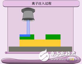
The wafer substrate is a pure silicon material that is non-conductive or extremely conductive. In order to have conductivity in the chip, a small amount of impurities, usually arsenic, boron, and phosphorus, must be incorporated into the wafer. Doping can be carried out in a diffusion furnace or by ion implantation. Some advanced applications are doped with ion implantation. In fact, the main purpose is to generate N-channel or P-channel. This doping process creates all the transistors and circuit connections to each other. No transistor has an input and an output, and the two ends are called ports.
Ion implantation has medium current ion implantation, high current/low energy ion implantation, and high energy ion implantation, which are suitable for different application requirements.
Chemical mechanical polishing
Chemical mechanical polishing (chemical machine polishing, CMP) and mechanical polishing with abrasive substances and chemical polishing of acid and alkali solutions can achieve a comprehensive planarization of the wafer surface for subsequent film deposition. get on. In a hard device of a CMP process, a polishing head is used to press a wafer onto a polishing pad and drive the wafer to rotate, while the polishing pad rotates in the opposite direction. When grinding is performed, a slurry composed of abrasive particles is placed between the wafer and the polishing pad.
Again and again, from this step, the layer will continue to be added, a layer of silicon dioxide added, and then photolithographically applied. Repeat these steps, and then there is a multi-layered stereo architecture, which is the budding state of the processor you are currently using. Conductive connections between the layers are carried out using a metal coating technique between each layer.
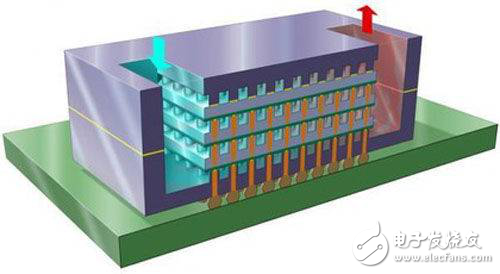
This is the internal structure of the chip, and it looks like a building. Wafer Metrology Wafer Metrology In the chip manufacturing process, in order to ensure that the wafer is processed according to the predetermined design requirements, a large number of inspections and measurements must be performed, including the measurement of the on-chip width, the measurement of the thickness of each layer, and the surface topography of each layer. Measurements, as well as measurements of some of the electronic properties of the various layers.
With the continuous development of semiconductor processes and manufacturing technologies, these tests have become an indispensable part of improving mass production and yield. In the copper interconnect process, the use of finer linewidth techniques and low-k dielectric materials requires the development of more sophisticated test equipment and new test methods.
The testing mainly includes three types: optical detection, thin film detection, and critical dimension scanning electronic detection (CD-SEM). An important development in wafer inspection is the integration of multiple measurement methods into one process equipment.
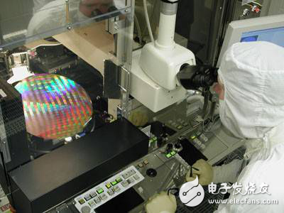
Wafer Probe Test This test is used to judge whether the chip is good or bad. The wafer probe test is a needle test on each chip (Die) on a finished wafer. When testing, the wafer is fixed on a vacuum suction chuck and is connected to a very thin probe. A probe that is as thin as a hair is in contact with each solder joint of the chip. During the test, the electrical performance and circuit function of each chip are detected. Unqualified dies will be marked, and then when the chip is cut into individual chip granules, the unqualified chip particles marked with marks will Be eliminated. Data on probe detection is now available to aid in yield improvement in wafer fabrication.
Chip Packaging (Assembly & Packaging)
The chips on the wafer are cut into individual chips here and then packaged so that the chips are finally placed on the PCB. The equipment needed here includes a wafer cutting machine, a die bonder (packaging the chip into the lead frame), a wire bonder (which is responsible for connecting the chip to the lead frame, such as gold wire bonding and copper wire bonding). Different types of leads are used in the wire bonding process: gold (Au), aluminum (Al), copper (Cu), each of which has its advantages and disadvantages, which are bonded by different methods. With the advent of multi-layer packages and even 3D package applications, the demand for ultra-thin wafers is also increasing. The chip was completed, and in the hands of the electrician, after a skilled welding process, it was embedded on the PCB and eventually became the heart of the electronic product.
Resolver is a kind of commonly used angle detection component, because of its simple structure, reliable operation, and its accuracy can meet the general detection requirements

Resolver
Resolver,Encoder Troubleshooting Resolver,Custom Resolver,Online Resolver
Yuheng Optics Co., Ltd.(Changchun) , https://www.yhencoder.com