Embedded System PDA Smartphone Design
I. Introduction
This article refers to the address: http://
With the rapid development of the handheld communication device market, the functions of mobile phones are gradually increasing. Nowadays, mobile phones are not only handheld devices for voice communication, but also an embedded communication platform that integrates additional functions such as SMS, MMS, Internet access and mobile office.
A phone that integrates these features is called a smartphone. In recent years, the speed and functionality of embedded processors have been greatly improved, making many applications that were previously only available on PCs now available on handheld devices. At present, the smartphones on the market mainly use Microsoft's Pocket PC, Palm OS and other commercial operating systems, but the open programs of these operating systems are not high enough, which limits the porting of many third-party applications. In order to enable the smart phone to provide a more open embedded platform for third-party application software, I have done a more in-depth study on the smart phone system, and proposed a Linux operating system, Motorola's MX1 as a microprocessor. Design and implementation of a smartphone system using Wavecom's Q2403A as the RF module.
Second, the introduction of smart phones (PDA)
The PDA is an abbreviation of Personal Digital Assistant, which literally means "Personal Digital Assistant." This handheld device combines computing, telephony, fax, and networking functions. It can be used not only to manage personal information (such as contacts, plans, etc.), but more importantly, it can browse the Internet, send and receive emails, send faxes, and even use it as a mobile phone. It is especially important that these features are implemented wirelessly. Of course, not all PDAs have all of the above features; even if they are available, they may not be implemented due to lack of corresponding services. However, it can be foreseen that the trend and trend of PDA development is the integration of computing, communication, network, storage, entertainment, e-commerce and other multi-functional.
PDAs are generally not equipped with a keyboard, but with handwriting or voice input. The operating systems used by PDAs mainly include Palm OS, Windows CE and EPOC.
Third, personal PDA needs analysis
As a 3C smart phone integrated into a terminal model, in addition to the communication function, it can realize many functions of computer and consumer electronics products, and has the advantages of small size, portability and versatility. After installing the application software, It can meet the differentiated needs of different consumers anytime and anywhere, and thus has the unique advantage that other products are irreplaceable.
Advances in IC technology have made it possible to develop and implement smart phones. In order to shorten the product design cycle, there are advanced SOC design concepts, 65nm or even narrower linewidth process technology. BGA, CSP, MCP and SI advanced packaging technologies and concepts are all intelligent. The technical advancement, functional realization and performance improvement of mobile phones provide strong and favorable support.
3G is about to start, and the bandwidth is significantly improved, which provides a strong guarantee for the smooth implementation and performance improvement of many new functions of the smartphone. For example, a smart phone with DMB (Digital Multimedia Broadcasting) function is difficult to implement on 2G and 2.5G. Even if it is implemented, the effect will be much worse. The clarity of the picture and the smoothness of playback are questionable, and all this is on the 3G network. It is not a problem.
Smartphones are facing unprecedented opportunities for development and convenience. With the improvement of consumer awareness and the development of usage habits, the sales share of smartphones in the entire mobile phone market will increase significantly. In the next five years, it will be from the current 6 The increase in % to around 20% will be accompanied by huge business opportunities in all aspects of the smartphone industry chain.
Fourth, the hardware design of the smart phone (PDA) system
The main parameters:
CPU: arm920T 200MHz (Motorola MC9328MXL);
Display: AU 3.5" Reflective TFT LCD with LED front light 65,536 colors;
ROM: 32MB Flash;
RAM: 64MB SDRAM;
Sound effects: Built-in mono microphone, built-in mono speaker, stereo headphone jack;
Touch screen: resistive touch screen;
SD/MMC: 1 SD card slot, MMC Ver3, 1.0 standard SDMC;
USB: USB 2.0 main, slave port;
Infrared: IrDA, 115Kpbs;
Serial port: RS-232 port;
LED: Red (charging indication), green (software running or battery fault indication)
Power Management: Full featured - Sipports Run, Idle and Sleep modes
Reset: set the reset switch;
Battery: 3.7V lithium ion battery
Physical size: motherboard size is 65x53x5.5mm
Power adapter: 5V DC;
External connectors: Possible integration, CF card, Sensor, Bluetooth, SIM Card, others
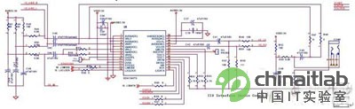
The hardware design of the smartphone system is shown in Figure 1. The design uses Motorola's MX1 (MC9328) high-performance 32-bit microprocessor, Wavecom's Q2403A wireless transceiver module to achieve smart phone GSM calls, GPRS Internet access and other PDA applications.
1 microprocessor
The MC928MX1 (hereafter referred to as MX1) is Motorola's first MCU based on the ARM core, mainly for high-end embedded applications. The internal arm920T core is used, and integrated controllers such as SDRAM/Flash, touch LCD, USB, bluetooth, multimedia flash card (MMC), and CMOS camera are integrated. For more information on MX1, interested readers can refer to http:// The smallest system developed as an application must include RAM (program run space), Flash (store target code), and serial interface (for debugging and downloading programs). The MX1 provides six chip select terminals (CS0~CS5) with a built-in SDRAM controller and a data width of 32 bits. In this system, two 8M×16-bit SDRAMs and two 4M×16-bit synchronous flash memories are used, which are respectively connected to the lower 16 bits and the upper 16 bits of the data line.
2 memory system
The physical essence of memory is one or more sets of integrated circuits with data input and output and data storage functions, used to act as a device cache or to store fixed programs and data. The memory can be classified into a read only memory (ROM) and a random access memory (Random Access Memory) according to the function of storing information. Solid-state storage in embedded systems generally does not use E2PROM, but uses Flash memory.

The following figure shows the composition of the memory system:
The following figure shows the schematic of the Flash memory section:
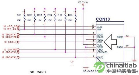
SD memory card circuit:
3. Power supply, clock and reset circuit
1. Power
The power section provides power to the entire system. The key issue in the power section is low-power design issues. Low-power measures typically include lowering the voltage, lowering the clock frequency, selecting low-power devices, and more. The power supply of this system is provided by battery power and mains power. The battery power supply has low power consumption, stable power supply, and good interference performance, but the peak performance is not good. The mains supply should have the corresponding AC-DC adapter, and the corresponding linear regulator should be configured on the system for DC-DC conversion.
The following figure shows the schematic diagram of the system power circuit:

2. Clock
Commonly used clock signals are RC clocks, crystal oscillator clocks, phase-locked loop multiplier clocks, and so on. In this system, the way to select OM[3:2] is grounded, that is, the external oscillator is used to provide the system clock. The external oscillator consists of a 12MHz crystal and two 15pF trimmer capacitors.
The following figure shows the schematic diagram of the clock circuit:

3. Reset
The design of the reset circuit is commonly used for RC reset, dedicated circuit reset, software reset, and so on.
The following figure shows the schematic diagram of the reset circuit.

The operation of the clock when the system is initialized:
The initialization program code of the system should be initialized and detected by the system hardware.
The power supply part should be set according to the actual system requirements, and the power-off mode and the wake-up code should be turned off.
The clock part should be set according to the requirements of the phase-locked loop. The reference code is as follows:
......
Ldr r0,=LOCKTIME
Ldr r1,=0xffffff
Str r1,[r0]
Ldr r0,=MPLLCON
Ldr r1,=((M_MDIV<<12)+(M_PDIV<<4)+M_SDIV); Fin=12MHz, Fout=50MHz
Str r1,[r0]
4. LCD module
LCD (Liquid Crystal Display) displays, which are often referred to as liquid crystal displays, are characterized by low power consumption and small size, and are widely used in embedded systems. Common LCDs include TN (Twist Nematic), STN, TFT (Tin Film Transistor), and the like. The main parameters of the LCD are resolution, backlight, interface, color, refresh rate and so on.
LCD controller function module diagram:

The wires connected to the LCD are driven by 74LVC16245:

LCD controller hardware connection:

5. Ethernet interface chip
Ethernet is a baseband LAN technology developed by Xeros. It initially uses coaxial cable as the network medium and uses Carrier Multiple Access and Collision Detection (CSMA/CD) mechanism to achieve a data transmission rate of 10 Mbps. Although Ethernet was first developed by Xeros in the 1970s, the term Ethernet is now used more often to refer to various LANs that use CSMA/CD technology. Ethernet is designed to meet the needs of non-persistent network data transmission, and the IEEE 802.3 specification was developed in 1980 based on the original Ethernet technology. Ethernet version 2.0 was jointly developed by Digital Equipment Corporation, Intel, and Xeros and is compatible with the IEEE 802.3 specification.
In the Internet, Ethernet can be regarded as the most widely used data link layer protocol.
Today's operating systems are capable of supporting this type of protocol format at the same time.
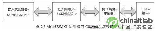
From a hardware perspective, an Ethernet interface circuit mainly by the MAC controller and the physical layer interface (Physical Layer, PHY) of two parts, the current common Ethernet interface chip, such as RTL8019, RTL8029, RTL8139, CS8900, DM9000 the like, Its internal structure also mainly contains these two parts. This system uses the CS8900 chip.
Ethernet interface design based on CS8900A:
RJ45 interface signal definition, and network cable connector signal arrangement
Ethernet 10/100Base-T interface:
1 TX+ Tranceive Data+ (Signal +) 2 TX- Tranceive Data- (Signal-)
3 RX+ Receive Data+ (receive signal +) 4 n/c Not connected (empty foot)
5 n/c Not connected 6 RX- Receive Data-
7 n/c Not connected 8 n/c Not connected (empty foot)
Network protocols in embedded systems: The general user's network application development is done at the application layer, and the underlying layer utilizes the off-the-shelf network protocol stack provided by the operating system.

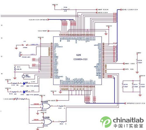
The connection-CPU part of the CS8900A:
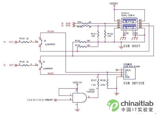
6. USB bus interface
The niversal Serial Bus is a new generation of standard interface bus jointly launched by Compaq, HP, Intel, Lucent, Microsoft, NEC and Philips. The bus is an off-board bus that connects peripheral devices and can connect up to 127 devices, making it easy to expand and configure external devices for microcomputer systems. There are several versions of the USB specification, the earliest version being the USB 0.7 version introduced in November 1994. The standard version of USB l.0 was introduced in January 1996. The goal is to provide a bidirectional, low-cost bus for low- and medium-speed peripherals with a data transfer rate of up to 12Mb/s.
With the enhancement of computer systems and peripherals performance and functionality, the amount of data to be processed is growing, in April 2000 launched a new USB specification -USB 2.0. In the new version, a data transfer rate of 480 Mb/s has been added to meet the demand for high-performance connectivity between increasingly sophisticated peripherals and PCs. USB 2.0 is a natural upgrade of USB, which provides higher bandwidth while retaining the original USB specification and is fully compatible with existing peripherals. Here is the USB2.0 interface.
7. Audio output and microphone circuit
The following figure shows the schematic diagram of the audio circuit:

The following figure shows the schematic of the microphone circuit:
8. Wireless transceiver module
This system uses WAVECOM's dedicated wireless transceiver module. It is a dual-band GSM module (EGSM900/1800MHz) designed and developed in accordance with the ETSI GSM Phase 2+ standard. With voice, GSM circuit data / fax, GPRS packet data, short messages and other functions. The module supports the AT command set and communicates with the MX1 via RS232.
Fifth, the software design of the smart phone (PDA) system
System analysis and software design are one of the difficulties in the implementation of smart phone systems. The advantages and disadvantages of design are related to the stability and scalability of the system. The design of the smartphone software system has become relatively complicated because of the need to balance the GSM voice control with other smartphone applications. The system design divides the software into three layers, as shown in Figure 2. The bottom layer is the operating system layer, which mainly implements the transplantation of the Linux operating system, including the bootloader bootloader, the driver of the LCD and other devices. The middle layer is the service program layer, which mainly includes the GUI server and the GSM/GPRS control server. The key to the design of smartphone systems lies in the implementation of various functional applications. The layered design of the smartphone software is conducive to the coordinated operation of each function, and also facilitates the development and debugging of the software.

1. Embedded Linux operating system
Linux was originally written by Linux Torvalds and released the source code is open, free use of the operating system. Later, with the addition of hundreds of programmers on the Internet, Linux became an operating system that supported almost all mainstream 32-bit CPUs. Its main features are: efficient and stable kernel, open source code, portability, reduction, support for multi-tasking, etc.
The Linux kernel used in this design is based on arm-Linux, and the boot program and power management control program conforming to the hardware design are written. For the hardware design of the system, hardware design drivers such as LCD and touch screen are written.
When the smartphone is based on the Linux operating system, the CPU is first initialized; then the device drivers are loaded, the memory and peripheral devices are initialized; and finally the service programs are started and the standby state is entered.
2. Service program design
The service programs in the smartphone system mainly include GUI Server and GSM/GPRS Server, which are the basis for the upper layer application.
GUI Server
In order to make the system support the complex interface applications such as browser and MMS, and have good scalability, the GUI Server design in this system adopts the client/server mode, and the graphics device is in the form of a dynamic link library. The interface is encapsulated, as shown in Figure 3.
The service process communicates with the application process using a message queue provided by Linux. The service process saves the description information of the system GUI environment, provides registration and some computing tasks for the application process, such as calculating the current cut domain content. In addition, it is also responsible for displaying the desktop. After the application is started, it first establishes a connection with the service process and interacts with it, and sends some description information of itself to the service process.
The service process and the application process implement the basic window display function by calling the dynamic library. The window tree and the clipping domain are defined in the dynamic library. For the service process or application, they are transparent and do not need to be managed. Because the service process runs in a different process space than the client process, although the same data is defined in the dynamic library, there is no conflict between them.

The design layered the functions encapsulated in the dynamic library. The function that directly outputs to the Framebuffer is at the lowest level of the system, which is the device context. Because each time a window is output, the design context must be established first. Therefore, the device context can always refer to the window structure. Naturally, it can also refer to the window clipping domain, and the output can be output within the scope of the clipping domain.
The graphics device interface is built on top of the device context, including points, lines, polygons, text, and so on. As mentioned above, before output, the device context is first established, ie the target of its output is the device context, not the window.
The upper layer of the graphics device interface is the application development interface, that is, the API layer. The desktop process and the client process implement system functions by calling API functions.
In addition, the system establishes an abstraction layer of inputs that shields different input devices.
GSM/GPRS Server multiplex communication server software
The GSM/GPRS Server multiplex communication server software is a daemon of telephone, short message and data services. It is responsible for responding to user operation events forwarded by the application and wireless communication module events obtained from the serial port, which is the core of the entire smart phone system. In this part of the work to achieve multi-link data communication, event priority discrimination, and in the implementation of data communication, to ensure access to telephones and text messages. The specific program device structure is shown in the figure.
3. Application design in the machine system
With the middle layer service program, the upper application can be ported and developed according to the interface provided by GUI Server and GSM/GPRS Server. In this design, the telephone control program, the management of short message transmission and reception, and the application of data energy are realized. The following is a telephone control program as an example to introduce the design and implementation of a smartphone application.
I divided the phone control program design into three operating states: PowerOn State, Idle State, and Execution State. Figure 5 shows the relationship between the three states and the conditions for entering each state.
The phone control program enters the Power-on State after the smart phone system is powered on and the GSM/GPRS Server is started. In the power-on state, the program first performs initialization work, communicates with the GSM/GPRS Server, and obtains the system status. After initialization, it enters the Idle State. In the idle state, the program loop waits for incoming calls from the GSM/GPRS Server and outgoing calls from the keyboard; when these events occur, the program enters the Execution State. In the execution state, the user performs voice communication, and after the call ends, the program returns to the idle state.
The system design has been successfully applied in practical engineering projects, and its feasibility and practicability have been tested in the actual application environment. In the next step, the CPU frequency of the system can be further improved, and the wireless communication module can be replaced with the 3G standard. In this way, a wider range of handheld device applications can be realized based on the design of the system.
Summary
Microprocessors using ARM technology intellectual property (IP) cores have been used in various product markets such as industrial control, consumer electronics, communication systems, network systems, and wireless systems. As a 16/32-bit high-performance, low-cost, low-power embedded RISC microprocessor, ARM microprocessors have become the world's most widely used embedded microprocessors. Through this embedded system smart phone (PDA) design, students with certain microcomputer-based principles have mastered the multi-faceted knowledge of developing embedded systems, and thus initially have the ability to design and develop ARM-based processor systems. Here, I would like to express my sincere gratitude to our teacher Huang Jianhua for bringing us such vivid teaching in the classroom. With his help, I realized the importance of the embedded system and made me feel the process of developing embedded systems. I have a lot of fun in the middle. However, learning the embedded system in a short period of 10 weeks is not enough. The theory and technology of embedded systems are developing with each passing day. This requires us to constantly explore and continue to explore in the future. Perfect, and because of the limited level and time rush, there is inevitably something wrong or wrong in the text. I hope the teacher can bear with me. I believe that only the effort is made and there is no fruit that cannot be received. I hope to learn the same subject of embedded systems! I am willing to work with scholars who are striving to be at the forefront of embedded systems development.
Ac Motor,Asynchronous Motor,Stepper Motor,Synchronous Motor
DC Motor Co., Ltd. , http://www.nbelectricmotor.com